We hope you are enjoying the summer! We are finalizing plans for the 2016 Fall AMIC annual meeting (save the date! September 8th, 2016 at the FLUNO center; interested in sponsorships?) with Erik Iverson, the new managing director of WARF, as the keynote speaker. This meeting will be co-hosted with the Wisconsin Materials Institute (WMI) and will feature a broader set of topics, including resources available for industry use across the UW system as well as new initiatives at the Madison campus such as the Grainger Institute for Engineering (GIE). The GIE will be more industry facing and will have thrust areas in Advanced Manufacturing, Smart Health Care, Materials Discovery, as well as in applications in Energy. The partnership among the MRSEC, WMI and GIE will enable faster, as well as potentially more industry targeted innovation, as well as seeding this growth with pipelines of students with opportunities for mentorship and recruitment. With this infrastructure being developed, your participation and involvement with the University will slowly grow the economy for Wisconsin and the nation.
Interestingly enough, Harvard Business review has an article discussing how interactions between industry and the University can be very beneficial for the company but also the university and the regional as a whole. (
https://hbr.org/2016/04/innovative-companies-get-their-best-ideas-from-academic-research-heres-how-they-do-it
). "The key, emphasizes
Jeff Welser
, a VP and Lab Director at
IBM's Almaden Research Center
is to be seen as an active participant and not just a spectator. "Being immersed is incredibly critical," he stresses. "You need to have people active at conferences, writing papers and helping the field advance. You have to put value in to get value out." So, we look forward to learning about any ideas you may have on how we can do more to foster this sort of relationship. In addition, UW President, Ray Cross, in an meeting with the Wisconsin Innovation Network (WIN) on June 28th, 2016 said, "stronger partnerships with industry leaders could help ensure the UW gets more support from the state going forward".
Best regards,
Felix Lu, and Erin Gill
AMIC, Co-Directors
|
 New technologies
Compact Spectrometer
THE INVENTION
A UW-Madison researcher has developed a more compact and easily manufactured optical spectrometer. Specifically, the new design includes a filter system that receives and modifies light beams according to frequency. It generates a set of uncorrelated and varying filter spectra over an extremely short optical path. Although the filter spectra are complex and appear largely random, they can be ordered into an absorption spectrum using compressed sensing techniques.
APPLICATIONS
- Telecommunications analysis and troubleshooting
- Chemical sensing
KEY BENEFITS
- New spectrometer is compact and robust.
- High sensitivity and resolution
- Low-cost and portable
- Provides an alternative to standard diffractive or Fourier transform spectrometry
- Efficient light analysis
- Extremely short external optical path
- Manufactured using conventional techniques
STAGE OF DEVELOPMENT
Accurate simulations have been performed. The researcher believes a 10-fold improvement in resolution is possible over similar devices. The on-chip array will contain approximately 400 probes and will operate in the visible light spectrum in the region typical of telecommunications applications.
Contact Information
For current licensing status, please contact Emily Bauer at
[email protected] or
(608) 262-8638.
|
2016 AMIC-WMI Annual meeting
Thursday, September 8th, 2016
Fluno Center, UW Madison campus
Keynote Speaker: Erik Iverson, Managing Director, WARF

with technical sessions on:
Materials and Manufacturing
Computation and Data Analytics
Material and Microbial Systems


|
|
|
September 28-29th, 2016 @ UW Stout
|
|
|
|
RM2N Fall Symposium
Monday, October 10th, 2016 UW Oshkosh
|
|
|
UW Engineering in the news
|
|
|
| Mikhail Kats(center) surrounded by his students. Photo: Sam Million-Weaver |
For anyone involved in imaging, the future is bright. Blindingly bright, in fact.
Today's imaging technologies allow highly sensitive cameras to detect even the faintest glimmers of light. Unfortunately, however, highly sensitive pieces of optical equipment are also highly susceptible to damage: Intense light beams overwhelm devices designed to detect single photons.
Here's one problem: As artificial eyes become more perceptive, high-powered light sources penetrate more spaces around the world. Even commonplace laser pointers can fry the optics of sensitive cameras, or temporarily blind pilots flying planes.
Somewhat like eyeglass lenses that darken in sunlight, transparent devices, called optical limiters, turn opaque on demand and could prevent intense beams from blinding sensitive detectors.
Read more:
https://www.engr.wisc.edu/blinded-light-no-designing-devices-protect-sensitive-imaging-systems/
|
|
|
| Billions of people worldwide lack clean_ safe water. Novel electrodes, at the heart of a UW2020 project co-led by UW-Madison soil scientist Joel Pedersen and chemist Robert Hamers, above, could enhance methods to inexpensively and efficiently inactivate bacteria and viruses in water. Photo: Jeff Miller |
Fourteen highly innovative research projects have been chosen for the first round of funding by the University of Wisconsin-Madison Office of the Vice Chancellor for Research and Graduate Education for the UW2020: WARF Discovery Initiative.
Sifting through 134 proposals from across the UW-Madison campus, reviewers identified ambitious, early stage research ideas and infrastructure investments in an effort to jump-start innovative interdisciplinary research projects.
"We have been inspired by the research ideas that have been put forward," says Marsha Mailick, UW-Madison vice chancellor for research and graduate education. "The goal of UW2020 is to support projects that could ultimately transform a field, solve a long-standing problem, contribute to social policy or launch a key new technology. We think we're off to a fantastic start."
Read more:
http://news.wisc.edu/uw2020-warf-discovery-initiative-proposals-selected/
|
 |
|
|
Using a unique method they developed, a team of UW Madison engineers has fabricated the world's fastest silicon-based flexible transistors, shown here on a plastic substrate. Courtesy of Jung-Hun Seo
|
One secret to creating the world's fastest silicon-based flexible transistors: a very, very tiny knife.
Working in collaboration with colleagues around the country, University of Wisconsin-Madison engineers have pioneered a unique method that could allow manufacturers to easily and cheaply fabricate high-performance transistors with wireless capabilities on huge rolls of flexible plastic.
The researchers - led by
Zhenqiang (Jack) Ma, the Lynn H. Matthias Professor in Engineering and Vilas Distinguished Achievement Professor in electrical and computer engineering, and research scientist Jung-Hun Seo - fabricated a transistor that operates at a record 38 gigahertz, though their simulations show it could be capable of operating at a mind-boggling 110 gigahertz. In computing, that translates to lightning-fast processor speeds.
Read more:
http://news.wisc.edu/with-simple-process-engineers-fabricate-fastest-flexible-silicon-transistor/
|
|
|
|
Deb Gilbert, director of research and development at Silatronix, oversees synthesis and evaluation of new battery electrolytes. David Tenenbaum |
Madison-made electrolyte going big at global battery manufacturer
Silatronix, a University of Wisconsin-Madison startup that has invented a safer electrolyte for the lithium-ion batteries used in phones, laptops and tablets, says its formulation has survived several years of evaluation and is now moving into pilot production at a major Japanese battery manufacturer.
The company cannot be identified, but it is known around the world, says Silatronix co-founder
Robert Hamers, a professor of chemistry at UW-Madison.
A lithium electrolyte is the heart of the market's lightest, most powerful batteries. But lithium batteries occasionally rupture and burn or explode.
The idea for the original Silatronix invention, a safer electrolyte, was hatched in one of those chance meetings beloved among advocates of scientific innovation. Hamers says
Robert West, a chemistry colleague, "was literally walking down the hall, and he asked me, 'Do you have anybody who can do electrochemical measurements?' I told him we measure the current-voltage relationships at solid-liquid interfaces all the time, and he started talking about a new electrolyte for a lithium ion battery he was developing."
Read more:
http://news.wisc.edu/madison-made-electrolyte-going-big-at-global-battery-manufacturer/
|
|
|
|
Professor Dane Morgan |
New material, picked by computers, could boost power of vacuum electronics
Modern tools like microwave ovens and X-ray machines that are powered by intense, focused beams of electrons are ubiquitous, but many of the materials in those devices have remained largely unchanged for decades.
Now, electrical and materials engineers at the University of Wisconsin-Madison have identified a substance that could vastly improve the technology.
This new material, a member of a broad class of compounds called perovskites, could boost the output power of the electron beam and enable long-range communications or remote sensing for a fraction of the current energy costs.
With a $1.3 million grant from the Defense Advanced Research Projects Agency, the researchers aim to synthesize large amounts of the material and further study its properties -- as well as search for even more applications.
Devices that may benefit from UW-Madison's perovskite work draw useful energy from streams of electrons flying through a vacuum, and therefore are called vacuum electronics. Vacuum electronic devices put electron energy to work for a broad array of functions, from accelerating particles in research reactors to detecting distant objects using radar to communicating with interstellar probes cruising past Pluto.
Read more:
https://www.sciencedaily.com/releases/2016/06/160614214556.htm
|
|
|
|
Evinrude's 250 horsepower E-TEC G2 (shown powering a bass boat) was designed with help from engine modeling software developed at the University of Wisconsin-Madison College of Engineering. Photo courtesy of BRP, Evinrude |
To understand what happens inside the cylinder of an outboard motor running at 5500 rpm, BRP/Evinrude got some help from an unlikely source: software code originally written to understand the motion of air after an atomic bomb explosion.
The physics of fluid flow are applicable in both cases, says
Rolf Reitz, a professor emeritus of mechanical engineering at the University of Wisconsin-Madison. In the 1970s, in response to the OPEC oil crisis, Reitz helped repurpose code written by the weapons group at Los Alamos National Laboratory for the auto industry.
The result became the basis for a package called KIVA that predicts and explains the highly complex events inside an engine's cylinder, allowing designers to reach the "sweet spot" of high power, good fuel economy and low emissions.
The cylinder is a complex place, says Paul Westhoff, a mechanical engineer at BRP/Evinrude in Sturtevant, Wisconsin. Westhoff led the computational fluid dynamic modeling during the "blank sheet of paper" design for the combustion cylinders in Evinrude's E-TEC G2 engines, introduced in 2014.
Read more:
http://news.wisc.edu/new-high-power-evinrude-outboard-built-with-uw-madison-software/
|
Since World War II, the U.S. has been an innovation superpower. In virtually every advanced field, whether it's information technology, biotechnology, agriculture, or renewable energy, America holds a leading position. Other nations may challenge in one field or another, but no one can match its depth and breadth.
To account for its success, many point to America's entrepreneurial culture, its tolerance for failure and its unique ecosystem of venture funding. Those factors do play important roles, but the
most important thing driving America's success has been its unparalleled scientific leadership.
While private companies employ some excellent scientists, most of America's scientific research is
publicly funded. Take a look at any significant innovation,
such as an iPhone, and you'll find that most, if not all, of the technology came from some government program. Google got its start from a federal grant. This is no accident, but the result of the national strategy that Vannevar Bush outlined in his 1945 report to President Truman, "
Science, The Endless Frontier" that led to government agencies such as The National Science Foundation (NSF), The National Institutes of Health (NIH), and the Defense Advanced Research Projects Agency (DARPA).
It has been this architecture that has driven America's technological leadership, funding everything from the first computers, the internet, GPS, laser scanners at stores and
most blockbuster drugs. Return on this investment is high,
estimated to be anywhere from 20% to 40%. So for companies looking to create revolutionary products, identifying and accessing cutting edge, exploratory research is a key competitive advantage.
As Bush
wrote in 1945: "New products and new processes do not appear full-grown. They are founded on new principles and new conceptions, which in turn are painstakingly developed by research in the purest realms of science."
|
|
|
|
|
Feedback from experiments, augmented dataset with four new alloys. Los Alamos National Laboratory
|
|
Machine Learning Accelerates Discovery of New Materials
Researchers recently demonstrated how an informatics-based adaptive design strategy, tightly
coupled to experiments, can accelerate the discovery of new materials with targeted properties, according to a recent paper published in Nature Communications.
"What we've done is show that, starting with a relatively small data set of well-controlled experiments, it is possible to iteratively guide subsequent experiments toward finding the material with the desired target," said Turab Lookman, a physicist and materials scientist in the Physics of Condensed Matter and Complex Systems group at Los Alamos National Laboratory. Lookman is the principal investigator of the research project.
"Finding new materials has traditionally been guided by intuition and trial and error," said Lookman."But with increasing chemical complexity, the combination possibilities become too large for trial-and-error approaches to be practical."
|
Why doesn't a spider's web sag in the wind or catapult flies back out like a trampoline? The answer, according to new research by an international team of scientists, lies in the physics behind a 'hybrid' material produced by spiders for their webs.
Pulling on a sticky thread in a garden spider's orb web and letting it snap back reveals that the thread never sags but always stays taut-even when stretched to many times its original length. This is because any loose thread is immediately spooled inside the
tiny droplets of watery glue that coat and surround the core gossamer fibres of the web's capture spiral.
This phenomenon is described in the journal PNAS by scientists from the University of Oxford, UK and the Université Pierre et Marie Curie, Paris, France.
The researchers studied the details of this 'liquid wire' technique in
spiders' webs and used it to create composite fibres in the laboratory which, just like the spider's capture silk, extend like a solid and compress like a liquid. These novel insights may lead to new bio-inspired technology.
|
| Materials, Advanced Manufacturing and Related topics |
|
|
| Applied SmartWeb (Source: Applied Materials) |
Manufacturing flexible electronics and coatings for a variety of products has some similarities to semiconductor manufacturing and some substantial differences, principally roll-to-roll fabrication, as opposed to making chips on silicon wafers and other rigid substrates. This interview is with Neil Morrison, senior manager, Roll-to-Roll Coating Products Division,
Applied Materials.
1. What are the leading market trends in roll-to-roll coating systems?
Neil Morrison: Several market trends are driving innovations in roll-to-roll technology and barrier films. One is the flexible electronics market where we see the increasing use of film-based components within displays for portable electronic devices such as smartwatches, smartphones, tablets and laptops.
The majority of these passive applications are for anti-reflection films, optical polarizers and hard coat protected cover glass films.
Examples of active device applications include touch sensors. Roll-to-roll vacuum processing dominates this segment through the use of low-temperature deposited, optically matched layer stacks based on indium tin oxide (ITO). Roll-to-roll deposition of barrier film is also increasing with the emergence of quantum dot-enhanced LCD displays and the utilization of barrier films in organic light-emitting diode (OLED) lighting.
In addition to the electronics industry, roll-to-roll technology is used for food packaging and industrial coatings. What's new today for food packaging is consumers want to be able to view the freshness of the food inside the packaging. Given this, the use of both aluminum foil and traditional roll-to-roll evaporated aluminum layers is slowly being phased into vacuum-deposited aluminum oxide (AlOx) coated packaging.
Within the industrial coatings market segment, significant growth is being driven by the use of Fabry-Perot color shift systems for "holographic" security applications, such as those used to protect printed currency from counterfeiting. This requires the use of electron-beam evaporation tooling to deposit highly uniform, optical quality dielectric materials sandwiched between two metallic reflector layers.
2. What are the leading technology trends in roll-to-roll coating systems?
Read more:
http://semimd.com/blog/2016/04/18/roll-to-roll-coating-technology-its-a-different-ball-of-wax/
Composite 3D Printer Has A New Way To Make High-Strength Woven Parts
This newly launched 3D printer can extrude woven fiber composite parts, resulting in glass, carbon fiber, or other aramid fibers suitable for the aerospace and automotive industries as well as other high-pressure environments.
EnvisionTEC announced the SLCOM 1 3D printer, the first commercial printer to use the patent pending process known as Selective Lamination Composite Object Manufacturing to create woven materials, on Tuesday. It works by building up composite parts layer-by-layer out of laminated thermoplastic composite fabric sheets. The sheets come in a roll, and EnvisionTEC is offering a variety of different types of materials. The printer can produce objects up to 24" x 30" and 24" in height.
"This represents a paradigm shift for manufacturing, especially where demanding mechanical and environmental properties can only be delivered from woven composites," said Al Siblani, CEO of EnvisionTEC. The company also commercialized the first DLP 3D printer on the market in 2002.
Researchers Open Hairy New Chapter in 3D Printing
|
|
| "It's very inspiring to see how these _hair-like_ structures occur in nature and how they can achieve different functions", says Jifei Ou, a graduate student in media arts and sciences at MIT. "We're just trying to think how can we fully utilize the potential of 3-D printing_ and create new functional materials whose properties are easily tunable and controllable." Pictured is an example of 3-D printed hair. Courtesy of Tangible Media Group, MIT Media Lab |
These days, it may seem as if 3-D printers can spit out just about anything, from a full-sized sports car, to edible food, to human skin. But some things have defied the technology, including hair, fur, and other dense arrays of extremely fine features, which require a huge amount of computational time and power to first design, then print.
Now researchers in MIT's Media Lab have found a way to bypass a major design step in 3-D printing, to quickly and efficiently model and print thousands of hair-like structures. Instead of using conventional computer-aided design (CAD) software to draw thousands of individual hairs on a computer - a step that would take hours to compute - the team built a new software platform, called "Cilllia," that lets users define the angle, thickness, density, and height of thousands of hairs, in just a few minutes.
Using the new software, the researchers designed arrays of hair-like structures with a resolution of 50 microns - about the width of a human hair. Playing with various dimensions, they designed and then printed arrays ranging from coarse bristles to fine fur, onto flat and also curved surfaces, using a conventional 3-D printer. They presented a paper detailing the results at the Association for Computing Machinery's CHI Conference on Human Factors in Computing Systems in May.
Read more at: http://www.rdmag.com/news/2016/06/researchers-open-hairy-new-chapter-3d-printing
|
Putting pressure on 3D-printed structures
|
|
|
|
A snapshot from a finite element simulation where the color scale indicates the material velocity and deformation of the lattice as the compression wave travels from left to right. Credit: Lawrence Livermore National Laboratory
|
|
Through a series of dynamic compression experiments on additively manufactured (AM) structured lattices, a Lawrence Livermore National Laboratory team, supported by colleagues at Los Alamos National Laboratory, has found that the assemblies have unique properties not exhibited by disordered cellular materials.
During the experiment, elastic deflection of the structure occurred ahead of the compaction front and in turn the AM lattice materials supported a precursor wave that has not been seen in disordered materials, such as traditional open-cell stochastic foams, which have a comparable density.
This research allows scientists to build accurate models of AM-structured materials under dynamic loading. The study (link is external) is published in the June 20 edition of Scientific Reports.
Read more:
http://phys.org/news/2016-06-pressure-3d-printed.html
|
|
Photonic and Electronic Materials & Devices
|
In the world of nano-scale technology, where work is conducted at the atomic level, even the smallest changes can have an enormous impact. And a new discovery by a University of Alberta materials engineering researchers has caught the attention of electronics industry leaders looking for more efficient manufacturing processes.
Triratna Muneshwar, a postdoctoral fellow in the Department of Chemical and Materials Engineering and Ken Cadien, a materials engineering professor, have developed a new method of making thin films-
materials that are essential in today's computers and electronic devices-by adapting current atomic layer deposition techniques.
Atomic layer deposition (ALD) is exactly what the name implies. Thin films are coated with molecule-thin layers of materials like zinc, silicon, nitrogen, and so on. In the manufacturing process, the film is placed inside a small chamber and prepared by being treated with a "sticky" precursor layer. Gasses are then pumped inside, coating and chemically binding to receptors on the precursor layer.
The problem is that some of the molecules coming to rest on top of the precursor layer are so large that they block other receptor points. It's like five people taking up 10 seats on a bus.
However, Muneshwar observed that those large molecules almost immediately shed ligands that do not connect to the precursor layer, freeing up previously blocked receptors. But by this time, the gas has been pumped out of the chamber and cannot be used a second time. "Although few strategies have been proposed to recycle this unreacted gas, residual impurities within remains a serious concern," he notes.
Read more:
http://electroiq.com/blog/2016/03/molecular-scale-ald-discovery-could-have-industrial-sized-impact/
|
Optics breakthrough to revamp night vision
|
|
|
When light falls on a very thin, uniform layer almost all of it is reflected (right-hand arrows). By etching thin grooves in the film, the light is directed sideways and almost all of it is absorbed (left-hand arrows) even though the amount of material is very small. Insets show electron micrographs of the structuring. The absorbing layer is only 0.041 um thick. Credit: Dr Thomas P. White, Australian National University.
|
A breakthrough by an Australian collaboration of researchers could make infra-red technology easy-to-use and cheap, potentially saving millions of dollars in defence and other areas using sensing devices, and boosting applications of technology to a host of new areas, such as agriculture.
Infra-red devices are used for improved vision through fog and for night vision and for observations not possible with
visible light; high-quality detectors cost approximately $100,000 (including the device at the University of Sydney) some require cooling to -200°C.
Now, research spearheaded by researchers at the University of Sydney has demonstrated a dramatic increase in the absorption efficiency of
light in a layer of semiconductor that is only a few hundred atoms thick - to almost 99 percent light absorption from the current inefficient 7.7 percent.
Read more:
http://phys.org/news/2016-05-optics-breakthrough-revamp-night-vision.html
|
New track for converting waste heat to electricity
|
|
| A high-entropy alloy imaged with a scanning electron microscope. Credit_ Sheng Guo |
Huge amounts of energy are lost every day in the form of waste heat. Now an interdisciplinary project at Chalmers has found that a special class of material - high-entropy alloys - can open the door to efficient heat recycling.
Boosting energy efficiency is an important element of the transition to a sustainable energy system. There are big savings to be made. For example, less than half the energy content of diesel is actually used to power a diesel truck. The rest is lost, mostly in the form of heat. Many industrial processes also deal with the problem of excessive
waste heat.
That's why many research teams are working to develop
thermoelectric materials -
materials that can convert waste heat into energy. But it's no easy task. To efficiently convert heat to electricity, the materials need to be good at conducting electricity, but at the same time poor at conducting heat. For many materials, that's a contradiction in terms.
"One particular challenge is creating thermoelectric materials that are so stable that they work well at high temperatures," says Anders Palmqvist, professor of materials chemistry, who is conducting research on thermoelectric materials.
He first met materials scientist Sheng Guo at an interdisciplinary workshop on materials for energy applications at Chalmers. Guo works with a fairly new type of material called high-entropy alloys, at the Department of Materials and Manufacturing Technology at Chalmers. High-entropy alloys typically consist of at least five elements, usually metals, at fairly similar quantities. They are stable even at
high temperatures, and the characteristics of the alloys can be manipulated by varying the components or the quantities of the components.
Read more:
http://phys.org/news/2016-06-track-electricity.html
|
Making Electronics from Unrefined Coal
|
|
| A sample of pulverized coal with several test devices made by MIT researchers. (Image courtesy of MIT.) |
Engineers are aiming to change the way coal is used by repurposing it from combustible fuel into electronic devices for a variety of industries, including energy, aviation and healthcare.
Even though coal has been one of the most widely used substances for centuries, its bulk electronic and optical properties have never been studied for the express purpose of creating electronic devices.
Recently, new research demonstrated how unrefined coal can be used to create a simple electric heating device for use in defrosting car windows or airplane wings. This initial application lead to the first ever detailed characterization of the chemical, electric and optical properties of thin films made from four different types of coal: anthracite, lignite and two bituminous types.
Read more:
http://www.engineering.com/DesignerEdge/DesignerEdgeArticles/ArticleID/12199/Making-Electronics-from-Unrefined-Coal.aspx
|
Liquid Crystals Open New Route to Planar Optical Elements
|
|
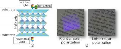
| Schematic illustration (left) and photos (right) of a standard cholesteric liquid crystal device. The green bars in the left figure are guides indicating positions with the same helix phase. Cholesteric liquid crystals reflect circularly polarized light with the same handedness as the helical structure and with wavelength fulfilling the Bragg condition (refractive index, helical pitch). In the right figure, purple light with right circular polarization is reflected. Source: Osaka University |
Researchers at Osaka University developed a technology to control the light wavefront reflected from a cholesteric liquid crystal - a liquid crystal phase with a helical structure. Although known for their ability to Bragg-reflect light, cholesteric liquid crystals could only be used as flat mirrors, reflecting light at the same angle as the incident angle. The new technology enables planar optical components to be made with functionality by design, contributing to the miniaturization of catoptrics devices.
The cholesteric liquid crystal is a liquid crystal phase in which the constituent rod-like molecules spontaneously form a helical structure (Fig. 1). Owing to its structure, cholesteric liquid crystals exhibit Bragg-reflection for circularly polarized light with the same polarization handedness as the helix, over a wavelength range determined by the refractive index and the helical pitch. Their characteristic optical properties, as well as the fact that structure is formed by self-organization, have made cholesteric liquid crystals attractive for use as circular polarizers, light reflectors, and electronic papers. However, their ability to function only as a flat dielectric mirror in which light must follow the law of reflection posed a limit on the performance they could achieve, and hence usage of devices based on these materials.
Read more:
http://www.rdmag.com/news/2016/06/liquid-crystals-open-new-route-planar-optical-elements?et_cid=5346606&et_rid=614174443&type=cta&et_cid=5346606&et_rid=614174443&linkid=http%3a%2f%2fwww.rdmag.com%2fnews%2f2016%2f06%2fliquid-crystals-open-new-route-planar-optical-elements%3fet_cid%3d5346606%26et_rid%3d%%subscriberid%%%26type%3dcta
|
3D printing of complex micro-objectives
|
|
| Complex triplet lens by femtosecond 3D printing on a single mode optical fiber. Source: University of Stuttgart |
3D printing has revolutionized the manufacturing of complex shapes in the last few years. Using additive depositing of materials, where individual dots or lines are written sequentially, even the most complex devices could be realized quickly and easily. This method is now also available for optical elements.
Researchers at
University of Stuttgart in Germany have used an ultrashort laser pulses in combination with optical photoresist to create optical lenses that are hardly larger than a human hair. PhD student Timo Gissibl in the group of Prof. Harald Giessen at the 4th Physics Institute printed micro-objectives with a diameter and height of only 125 µm, even on optical fibers. This permits the construction of novel and extremely small endoscopes which are suited for smallest body openings or machine parts that can be inspected. The optical design was realized in the Stuttgart Research Center for Photonics Engineering by Ph.D. student Simon Thiele from the group of Prof. Alois Herkommer at the Institute of Technical Optics in Stuttgart.
Timo Gissibl also printed optical free form surfaces and miniature objectives directly onto CMOS image chips, which thus create an extremely compact sensor. Using such optics, smallest cameras from drones that are not larger than a bee are possible. Also, the smallest sensors for autonomous cars and robots are conceivable. Even smallest body sensors and surround-cameras for cellphones could be realized.
The Stuttgart researchers believe that 3D printing of optics is going to open an entire new era of optics manufacturing. "The time from the idea, the optics design, a CAD model, to the finished, 3D printed micro-objectives is going to be less than a day", states Harald Giessen. "We are going to open potentials just like computer-aided design and computer-integrated manufacturing did in mechanical engineering a few years ago".
Read more:
http://www.materialsviews.com/3d-printing-complex-micro-objectives/?elq_mid=10540&elq_cid=3733327
|
|
Microstructured Thin FIlms and Coatings
|
Composite metal foams (CMFs) are tough enough to turn an armor-piercing bullet into dust on impact. Given that these foams are also lighter than metal plating, the material has obvious implications for creating new types of body and vehicle armor - and that's just the beginning of its potential uses.
Afsaneh Rabiei, a professor of mechanical and
aerospace engineering at NC State, has spent years developing CMFs and investigating their unusual properties. The video seen here shows a composite armor made out of her composite metal foams. The bullet in the video is a 7.62 x 63 millimeter M2 armor piercing projectile, which was fired according to the standard testing procedures established by the National Institute of Justice (NIJ). And the results were dramatic.
"We could stop the bullet at a total thickness of less than an inch, while the indentation on the back was less than 8 millimeters," Rabiei says. "To put that in context, the NIJ standard allows up to 44 millimeters indentation in the back of an
armor." The results of that study were published in 2015.
But there are many applications that require a material to be more than just incredibly light and strong. For example, applications from space exploration to shipping nuclear waste require a material to be not only light and strong, but also capable of withstanding extremely high temperatures and blocking radiation.
Read more:
http://phys.org/news/2016-04-metal-foam-obliterates-bullets.html
http://www.rsc.org/chemistryworld/2016/04/bulletproof-armour-composite-metal-foam
|
Researchers at North Carolina State University have developed a new metallic bubble wrap that is lighter, stronger and more flexible than sheet metal and more heat- and chemical-resistant than plastic or other polymer-based bubble wraps. Potential applications include automobile body panels, the wing edges of airplanes, suitcases, helmets and cases for computers and other electronic devices.
"This material does exactly what sheet metal and other bubble wraps do, but better," said Dr. Afsaneh Rabiei, professor of mechanical and aerospace engineering and the lead researcher on the project. "And it won't cost businesses and consumers very much because producing it requires just a few steps."
Rabiei developed the metallic bubble wrap to offer protection in areas that are only a few millimeters thick. To be effective, such materials must be thin enough to fit inside tightly spaced product linings, flexible enough to withstand twisting and bending, and strong enough to protect the contents inside.
Read more:
http://phys.org/news/2013-07-metallic-big-benefits-materials.html
|
NRL Reveals Novel Uniform Coating Process of p-ALD
|
|
|
Image shows high magnification bright field transmission electron microscopy (TEM) image showing obvious delineation of alumina film and surface of particle. In this work, performed by NRL researchers, the growth per
cycle (GPC) during atomic layer deposition is compared for different batches of powder with average particle sizes ranging from nanometer (nm) to micrometer (m). Samples prepared after depositing thin alumina films _from 10 to 15 nm on tungsten powders using particle atomic layer deposition (p-ALD) were investigated with x-ray photoelectron spectroscopy (XPS) scanning and transmission electron microscopy (SEM) and TEM. Source: US Naval Research Laboratory
|
Scientists at the U.S. Naval Research Laboratory (NRL) have devised a clever combination of materials -- when used during the thin-film growth process -- to reveal that particle atomic layer deposition, or p-ALD, deposits a uniform nanometer-thick shell on core particles regardless of core size, a discovery having significant impacts for many applications since most large scale powder production techniques form powder batches that are made up of a range of particles sizes.
"Particle atomic layer deposition is highlighted as a technology that can create new and exciting designer core/shell particles to be used as building blocks for the next generation of complex multifunctional nanocomposites," said Dr. Boris Feygelson, research engineer, NRL Electronics Science and Technology Division. "Our work is important because shell-thickness is most often a crucial parameter in applications where core-shell materials can be used to enhance performance of future materials."
|
Borides are among the hardest and most heat-resistant substances on the planet, but their Achilles' Heel, like so many materials', is that they oxidize at high temperatures. Oxidation is the chemical reaction commonly known as corrosion or rusting -- it can signal the end for a material's structural integrity. But researchers from Drexel University, Linkoping University in Sweden and Imperial College London have produced an aluminum-layered boride whose unique behavior at high temperatures keeps it one step ahead of nature's slow march toward high- temperature chemical degradation.
So impressive is their perceived durability, that borides are used as coatings for surfaces that must survive the harshest environments - from the inside of combustion engines to cutting tools for hard metals. But, according to Michel Barsoum, PhD, distinguished professor in Drexel's College of Engineering who is the lead author of research recently published in
Scientific Reports, we can make borides better.
|
|
Characterization of Advanced Materials
|
|
|
|
| Figure 1. Specific strength vs. elongation to failure for a range of Mg alloys. Red diamond (LX41) blue square (Mg-30Li) further symbols correspond to literature data for other hot-rolled Mg alloys and are explained in the original publication Y. Estrin et al., Materials Letters 173-252, 256 (2016). |
|
Developing increasingly lighter and stronger alloys for engineering applications is an ongoing - and never ending - endeavor of materials scientists. Magnesium alloys - the lightest structural metallic materials available - are therefore in the focus of research. Alloying magnesium with an even lighter element, lithium, is an attractive pathway to develop new ultralight alloys with a high specific strength, defined as the strength to density ratio.
A record specific strength of Mg-30 at. % Li alloy reported recently [W. Xu et al., Nature Materials 14, 1229-1235 (2015)] has been celebrated as a great success on this path. This success has now been followed by a development in which an even higher specific strength and almost the same high ductility has been achieved with an alloy of the Mg-Li system with a lower lithium content and some Ca addition: a tertiary alloy Mg-4Li-1Ca (concentrations in wt. %) [Y. Estrin et al., Materials Letters
173
, 252-256 (2016)]. A remarkable fact is that the superior mechanical performance of alloy Mg-4Li-1Ca (LX41) demonstrated in Fig. 1 was achieved using a rather simple processing route, which is amenable to industrial practice. It involves hot rolling at two different temperatures (two-step rolling) to a total thickness reduction of just 60% and subsequent 30 min annealing, referred to as TA30 treatment. The property profile the alloy acquires after this treatment is extraordinary. The authors relate these superior properties of LX41 to microstructure and texture produced by this processing. A further advantage of the new alloy in TA30 condition is its record strain hardening ability at room temperature, i.e. the difference between the ultimate tensile strength (UTS) and the yield strength (YS) illustrated in Fig. 2. This means that the material is easy to form and becomes stronger in the process of forming, which is advantageous for future service.
Read more:
http://www.materialsviews.com/31702-2/?elq_mid=9579&elq_cid=3733327
|
Researchers at MIT are seeking to redesign concrete - the most widely used human-made material in the world - by following nature's blueprints.
In a paper published online in the journal Construction and Building Materials, the team contrasts cement paste - concrete's binding ingredient - with the structure and properties of natural materials such as bones, shells, and deep-sea sponges. As the researchers observed, these biological materials are exceptionally strong and durable, thanks in part to their precise assembly of structures at multiple length scales, from the molecular to the macro, or visible, level.
From their observations, the team, led by Oral Buyukozturk, a professor in MIT's Department of Civil and Environmental Engineering (CEE), proposed a new bioinspired, "bottom-up" approach for designing cement paste.
"These materials are assembled in a fascinating fashion, with simple constituents arranging in complex geometric configurations that are beautiful to observe," Buyukozturk says. "We want to see what kinds of micromechanisms exist within them that provide such superior properties, and how we can adopt a similar building-block-based approach for concrete."
Read more:
http://news.mit.edu/2016/finding-new-formula-for-concrete-0526
|
|
|
|
Dimethyl methylphosphonate, a sarin simulant, sits inside the supramolecular cage, partially quenching its fluorescence
|
Organophosphorous chemical weapons, such as
sarin and
soman, interfere with signals between nerve cells, and have recently been used to deadly effect in places such as Syria. Researchers are therefore trying to develop techniques that detect these chemical weapons in the environment, and destroy them.
Mike Ward and his group at the University of Sheffield in the UK may have found a way, using self-assembled supramolecular cages - large, hollow molecular structures that can act as a host to smaller molecules. Such structures have been around for a while, but the ones made by Ward are exciting because they can bind alkyl phosphonates within them. Alkyl phosphonates have the same basic size and shape as the chemical weapons in question, but lack the reactive leaving group that makes them so dangerous so researchers often use them as chemical weapon simulants in the lab.
The host cages have a cobalt or cadmium dication at each vertex and a bis(pyrazolyl-pyridine) ligand along each edge. In water, the hydrophobic effect drives interactions between the cage and alkyl phosphonates. 'The interior surface is lined with CH groups from the ligands, which is an archetypal hydrophobic surface - oil and water don't mix for the same reason,' explains Ward. 'It thus acts as a haven for molecules that are not happy in water. For the guests, their alkyl chains provide the hydrophobic contribution to binding. We can see this because, as the size of the alkyl groups increases, binding gets stronger - even though the phosphonate bit stays the same in every case.' It is energetically favourable for this hydrophobic guest to enter the hydrophobic cavity because each guest displaces two bound water molecules, allowing them to form hydrogen bonds with each other, and increasing the total entropy by being free to move around.
Read more:
http://www.rsc.org/chemistryworld/2016/04/supramolecular-cage-chemical-weapons-sarin-hydrophobic-effect
|
|
|
|
Researchers at Oregon State University using new technology to control the formation and release of bubbles illustrate it with the letters (OSU) being printed on a substrate. Credit: Oregon State University |
Engineers at Oregon State University have found a new way to induce and control boiling bubble formation, that may allow everything from industrial-sized boilers to advanced electronics to work better and last longer.
Advances in this technology have been published in Scientific Reports and a patent application filed.
The concept could be useful in two ways, researchers say - either to boil water and create steam more readily, like in a boiler or a clothing iron; or with a product such as an electronics device to release
heat more readily while working at a cooler temperature.
"One of the key limitations for electronic devices is the heat they generate, and something that helps dissipate that heat will help them operate at faster speeds and prevent failure," said Chih-hung Chang, a professor of electrical engineering in the OSU College of Engineering. "The more bubbles you can generate, the more cooling you can achieve.
|
Microfluidics, or the manipulation of tiny volumes of liquids, is a widely used research technique for multiple applications including the high-throughput screening of blood and chemical samples. Conventional microfluidic devices are closed channels made from silicon or glass. They are produced in clean rooms with semiconductor fabrication technology, which is expensive and time-consuming. Paper microfluidics is an emerging field focused on creating inexpensive devices, with simple fabrication methods. The technique works by confining liquids within channels with different surface energies or wettability rather than physical walls. However, paper-based microfluidic devices thus far have largely been limited to working with relatively high surface tension liquids such as water. Many significant biological and chemical reactions are carried out in non-aqueous liquids, or at interfaces between immiscible liquids.
|
|
Biomaterials and Biotechnology
|
Will Raindrops Stick to a Spider Web's Threads?
|
|
|
Researchers from Sogang University were inspired by the way spider webs collect rain to develop a model to predict whether a falling droplet will stick to a thin fiber_ and how much water residue will remain on the fiber. (Credit, Wonjung Kim, Sogang University)
|
If you go out after a rain, you may notice spider webs glistening with water droplets. The soggy webs resemble human-made meshes for fog collection: They both have thin fibers that collect water from droplets in the air.
Now researchers from Sogang University in Seoul, South Korea have developed a model to predict whether a falling droplet will stick to a thin fiber, and how much water residue will remain on the fiber. They discuss their findings in this week's Physics of Fluids, from AIP Publishing.
"Engineers will apply our results to control the amount of liquid retained on fibers for water-collection from foggy air, air-filtration, and fiber-coating technologies," said Wonjung Kim, a mechanical engineer at Sogang University. "To our best knowledge, this is the first quantitative study of the remnant mass on the fiber after collision."
|
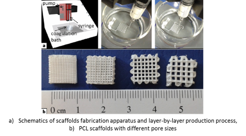
Can Polymers Regenerate Teeth?
 Various inflammations of the tissue around teeth, such as periodontitis, can result in tooth loss and degeneration of supporting connective tissue and alveolar bone. As such, a common goal for tissue engineering has been finding a way to regenerate and repair the inflamed tissues.
A potential solution relies on polymers, such as PCL (poly (ε-caprolactone)), which has been tested in recent clinical studies. Polymeric scaffolds made from PCL have shown that when they are combined with other materials, an enhanced healing of human intrabony effects can be achieved. Although PCL is a biocompatible material with good blend-compatibility and is widely investigated across different biochemical applications, it shows slow biodegradation which can limit its application for biodegradable implantation.
|

If you used any instruments in the Materials Science Center, Soft Materials Laboratory, or the Wisconsin Center for Applied Microelectronics, please remember to acknowledge MRSEC funded instruments and facilities in any publications (DMR-1121288). This will serve as a metric for how often MRSEC funded instruments are used and will help continue MRSEC support in future years. Thanks! If you have any questions, please contact
Felix Lu
.
|
|
|

The Soft Materials Lab
The Soft Materials Lab, housed in the basement of Engineering Hall, has a wide spectrum of instruments for characterizing soft materials. The lab is managed by
Anna Kiyanova who is available to answer all of your characterization questions.
C
 ontact:
Anna Kiyanova
[email protected]
(608) 263-1735
|
The Materials Science Center (MSC)
The Materials Science Center has a wide spectrum of electron, optical and physical characterization instruments and is fully staffed to help you with training and sample characterization.
Contact: 
Dr. Jerry Hunter
[email protected]
(608) 263-1073
|
The WCAM is a full spectrum micro/nano fabrication facility for processing and integrating devices in Silicon, III-V, group four, glass, plastic, materials. On site, fully-qualified and highly experienced staff are available to help you with your process development and answer questions.
 Contact: Contact:
Dan Christensen
[email protected]
(608) 262-6877
|

 Contact: Contact:
Dr. John Fournelle
Dept of Geology & Geophysics
University of Wisconsin-Madison
1215 W. Dayton St
Madison, WI 53706
(608) 262-7964 (office) 265-4798 (lab) 262-0693 (fax)
johnf*at*geology.wisc.edu
|
Biochemistry Optical Core
The Biochemistry Optical Core (BOC) provides state-of-the-art instrumentation for super-resolution light microscopic imaging. Expertise and advice is available for the design of experiments involving these techniques; and for the development of grants and manuscripts involving super-resolution and standard light microscopic technologies.
 Contact: Contact:
Dr. Elle Grevstad
Dept of Biochemistry
University of Wisconsin-Madison
440 Henry Mall
Madison, WI 53706
[email protected]
|
Paul Bender Chemical Instrumentation Center
The Paul Bender Instrument Center houses the Chemistry Department's major shared analytical instrumentation (magnetic resonance, and mass spectrometry, and X-ray diffraction). These instruments are maintained and updated by an expert staff that provides user training and data interpretation in support of Departmental research. The Center is located on the second floor of the Chemistry building.
 Contact: Contact:
Dr. Charles Fry
Dept of Chemistry
University of Wisconsin-Madison
(608)262-3182, Room: 2201A
|
|
Student tour groups of your facility
|
Industrial facilities tours?
Are you interested in showing off your facility to interested student groups? Do you want to increase exposure of what your company does to encourage higher application rates and get student interns? Hosting a tour might be a good start! Please contact
Felix Lu or
Erin Gill to initiate this!
|
|
Using our campus facilities
|
|
The Practical Side of Things
|
Non-destructive testing methods test mechanical and other properties without permanently altering the subject, which saves time and money in product evaluation.
There are many companies that sell non-destructive machines to test material properties but they rarely explain how their methods work. Eng-Tips Forums member "afronova"
posted the question, "Are there any good sites that inform about destructive and non-destructive material testing techniques?"
Well, afronova, there is now.
And so begins a three-part series on nine methods of non-destructive material testing. In part one, we discuss radiographic testing, ultrasonic testing and magnetic particle inspection.
Read more!
http://www.engineering.com/AdvancedManufacturing/ArticleID/12410/The-Basics-of-Non-Destructive-Material-Testing-Part-1.aspx
|
See this blog on "Producing Polymers and Plastics", which is sponsored by ThermoFisher Scientific (an AMIC member!)
Spraying automotive paints and coatings, and the application of paper coatings, are typical examples of industrial processes where the characterization of elongational properties is essential to optimizing product properties or production processes. Elongation flows occur in many industrial production and working processes where product flows experience cross sectional changes or are diverted.
Paints and coatings are usually highly structured fluids that consist of several different components, including additives that can be used to modify the surface tension, optimize the
thixotropic behavior, or improve finished appearance of the paint film. All these components contribute to the flow behavior of the final paint product.
Plastic is a leading material in the production and packaging of intermediate and finished goods. Few industries do not use plastics in their products, while consumers encounter plastics every day in the form of packaging, building/construction, transportation vehicles, medical equipment, scientific instruments, institutional products, furniture and furnishings, electronics, and apparel. The U.S. Environmental Protection Agency states that "in 2013, the United States generated about 14 million tons of plastics as containers and packaging, about 12 million tons as durable goods such as appliances, and almost 7 million tons as nondurable goods, such as plates and cups." Here is a brief overview of the most widely used plastics.
Read more!
http://acceleratingscience.com/polymers2plastics/rheological-investigations-of-automotive-and-paper-coatings-part-1/
|
|
|
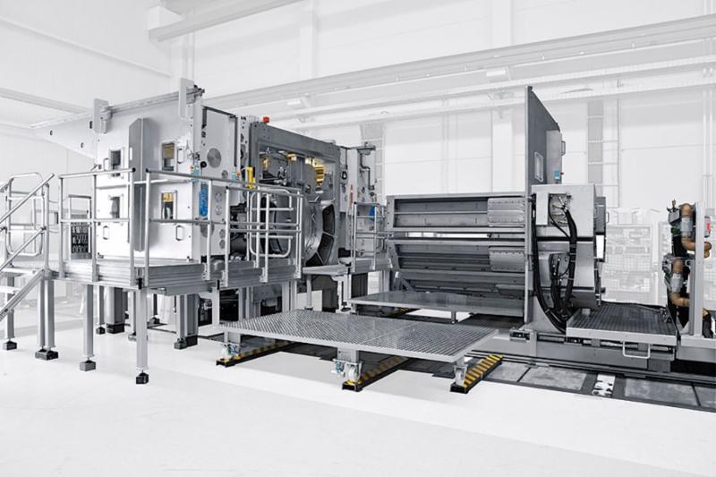
| Hot Dip Galvanizing _HDG_ Line with Cold Gauge and Hot Gauge measurements |
Spraying automotive paints and coatings, and the application of paper coatings, are typical examples of industrial processes where the characterization of elongational properties is essential to optimizing product properties or production processes. Elongation flows occur in many industrial production and working processes where product flows experience cross sectional changes or are diverted.
Paints and coatings are usually highly structured fluids that consist of several different components, including additives that can be used to modify the surface tension, optimize the
thixotropic behavior, or improve finished appearance of the paint film. All these components contribute to the flow behavior of the final paint product.
Proper coating of metal parts is an essential manufacturing step in the the automotive, aerospace, medical device industries. Paint, primer and organic coatings are applied to steel, galvanized steel, or aluminum strip to not only improve the appearance, strength, and durability of the metals but to help ensure that appropriate film thickness specifications are met so that the finished pieces function as intended and fit properly with other parts. Coil coating lines can benefit from
online thickness coating gauges for applications including:
- Weldable primer coatings with zinc particles applied to chromated or galvanized steel
- Ultra-thin coatings
- Wet measurement directly after the coaters
- Dry measurement made after drying ovens
- Chromate-free coatings for corrosion protection
- Oil and anti-fingerprint coatings
- See more at: http://acceleratingscience.com/polymers2plastics/a-primer-on-measurement-technologies-for-coating-weight-gauges/?utm_source=Plastics+%26+Polymers&utm_campaign=92f781a12c-RSS_EMAIL_POLYMERS&utm_medium=email&utm_term=0_da73239b7b-92f781a12c-208996797#sthash.tPduBoNT.dpuf
Read more!
http://acceleratingscience.com/polymers2plastics/a-primer-on-measurement-technologies-for-coating-weight-gauges/?utm_source=Plastics+%26+Polymers&utm_campaign=92f781a12c-RSS_EMAIL_POLYMERS&utm_medium=email&utm_term=0_da73239b7b-92f781a12c-208996797
|
The growth in popularity and acceptance of Fourier transform infrared (FT-IR) spectrometers for use in quality assurance (QA) laboratories and on manufacturing floors is one of the major developments affecting industrial environments in recent years. FT-IR spectroscopy offers almost unlimited analytical opportunities in many areas of production and quality control. It covers a wide range of chemical applications, especially in the analysis of organic compounds. In addition to its more classical role in qualitative analysis, its use in quantitative determinations has grown due to the improvements in signal-to-noise performance coupled with the development of advanced statistical analysis algorithms. Thanks to its compact design and ruggedness, the instrumentation can be located in the analytical laboratory or near the production line. Low cost, speed, and ease of analysis make FT-IR a method of choice for many industrial applications, including the analysis of polymeric materials.
Read more!
http://acceleratingscience.com/polymers2plastics/advantages-of-ft-ir-in-polymer-manufacturing/?utm_source=Plastics+%26+Polymers&utm_campaign=2b78f83a7c-RSS_EMAIL_POLYMERS&utm_medium=email&utm_term=0_da73239b7b-2b78f83a7c-208996797
|

Any number of medical, industrial and analytical applications requires the detection of light. Chemiluminescence, bioluminescence, fluorescence and atomic absorption are just a few, and all require a detector to convert the light into an electrical signal. There are four basic technologies that accomplish this task: photomultiplier tubes (PMTs), silicon photomultipliers (SiPMs), avalanche photodiodes (APDs), and silicon photodiodes.
The question of which detector to use is not a simple one. In applications where there is ample light, a photodiode is suitable. A PMT is the best choice where there are very weak signals. In other applications, however, the choice is not so clear. This article will examine detector characteristics, criteria for selection of a detector and amplifier performance, and hopefully, help you to choose.
Detector options
The PMT (Figure 1) consists of a photosensitive surface (photocathode), electron multipliers (dynodes), and a collection electrode (anode) within an evacuated glass or metal envelope. Light enters the input window and is absorbed by the photocathode. An electron is emitted from the cathode and accelerated to the first dynode by an applied voltage. The electron is accelerated to sufficient potential that, when it collides with a dynode, secondary electrons are produced. These secondary electrons are in turn accelerated to the next dynode, with the process being repeated until the electron cloud is collected at the anode.
Read more!
http://www.laserfocusworld.com/na/hamamatsu-corp/a-guide-to-choosing-the-right-detector.html#!/
|
for the 2016 AMIC-WMI annual meeting
Location:
Fluno Center,
601 University Ave, Madison, WI 53715
|
|
|
| Erik Iverson, Managing Director, WARF |
|
Keynote Speaker :
Erik Iverson, Managing Director, Wisconsin Alumni Research Foundation (WARF)
If you are interested in
sponsoring
the event or parts of the event (e.g. poster prizes, lunch, etc), please let us know!


|
|
 |
|