Happy 2016! We hope you had a good winter break with friends/family and had some well deserved downtime! In the fall, we held our annual meeting which many of you attended and have been busy setting up a new initiative and visiting current and prospective members. An event that will get everyone networking is the
upcoming Facilities Days Open House, on Thursday, January 28th at UW Madison in the Engineering Centers Building. We will be introducing not only the
College of Engineering core facilities, but also the
Biochemistry optical core and the
Paul Bender Chemical Instrumentation Center, as well as industry speakers. After the talks, there will be lunch, a poster session, and networking time as well as facilities tours with the industry reps at the instruments to run demos and help answer questions. We look forward to seeing you at this event!
Register here
!
One particular thing we like to talk about is how our AMIC members help the AMIC and the MRSEC by justifying to NSF their investment in the MRSEC.
By being AMIC members, you help justify the existence of and improvement of the shared instrumentation facilities, provide students with professional development opportunities and mentoring of senior capstone projects, give ideas for graduate student/postdoc student seed projects, provide internships, and inform students and faculty what current industry needs are. All these facets of regional collaboration and continued support help us become more effective as a consortium and tells the NSF that their continued funding is being put to good use for technology development, business growth and maturation of the economic infrastructure.
AMIC seed initiative
The new initiative we have been working on is a seed program that funds student and postdoc led projects. The funding comes from your AMIC member dues up to $15k per project. An executive committee composed of academic and industrial personnel evaluate proposals submitted by students/postdocs which may be in response to challenges and projects outlined by our industrial members. When project goals align with industrial needs, the company may put in optional matching funds to expand or deepen the scope of the project or better align it with their current interests. The call for proposals is schedule to begin in February of 2016. For more information, questions or comments, please contact us.
AMIC and RM2N meeting highlights
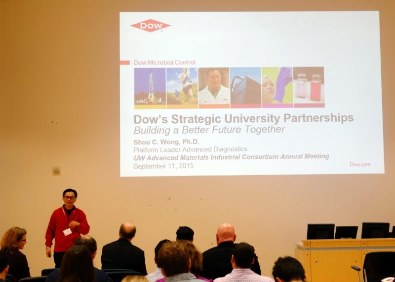
We had a very successful meeting with 122 registered participants, robust networking and fantastic talks from Shou Wong from DOW, Kevin Nelson from Bemis, Eric Nordberg from Brady, and Bryce Nelson from Sigma Aldrich. We also heard from Professor Dane Morgan about a very interesting initiative about a materials computational "skunkworks"
team of students to tackle large data sets related to current industrial interests. which We received helpful feedback and the parallel technical sessions seemed to resonate with the diverse audience. Pictures from the event are posted below. We would appreciate any additional feedback you have! This can be anything from the format to the operations, to the length of the event, to the color of the booklets. AMIC and the MRSEC were also present at the kickoff meeting for the Regional Materials and Manufacturing Network (RM2N) in Eau Claire. This was a great opportunity to tell regional industrial leaders about the resources and faculty expertise available in the expansive UW system. We encourage you to follow up with us if you have questions about the next meeting in Milwaukee!
Outreach We have been in contact and visited with several new companies in the past few months. These include a visit to the
Bemis innovation Center,
Sigma Aldrich,
Hydrite chemical company,
SSI Technologies,
Phoenix Nuclear Labs, and the
Global Water Center, and visits at UW Madison from
GKN Sinter metals,
Ensync Energy Systems,
Intuitive Biosciences, and
Subzero-Wolf.
All pictures, courtesy of Susann Ely,
Wisconsin Materials Institute.
|
|
Networking with students during the break
|
|
|
| Tour of the Soft Materials Lab (SML) |
|
|
| Kevin Nelson (L) from Bemis and Steve Goodman from Microscopy Innovations (R) |
|
|
| Dr. Shou Wong from DOW chemical giving the keynote address |
As always, if you have questions, suggestions or comments, please let us know!
Best regards,
Felix Lu and Erin Gill,
Co-Directors, UW AMIC
|
Are there topics of interest that you would like to see mentioned in the AMIC newsletter?
For example:
Properties of materials:
mechanical, structure, thermal, electric/magnetic, chemical, optical
Types of materials:
(i)
Metals (ferrous and non-ferrous) and alloys
(ii)
Ceramics
(iii)
Organic Polymers
(iv)
Composites
(v)
Semiconductors
(vi)
Biomaterials
(vii)
Advanced Material: glasses, meta-materials, etc.
Processing of materials:
welding, additive/subtractive manufacturing, casting, powder metallurgy, heat treatment, coatings, inks, refractory materials, porous materials,
Characterization of materials:
elemental/molecular ID/mapping
surface (roughness, topography, functionality, adhesion, etc.)
bulk properties / 3D mapping
This will help us focus the newsletter towards your interests.
Please let us know by
contacting us.
|
|
|
| Industry Sponsored Research Roadmap |
|
Recent Patents:
Polymer Coating for Cell Culture Substrates
The Wisconsin Alumni Research Foundation (WARF) is seeking commercial partners interested in developing a chemically defined culture surface with long-term stability.
OVERVIEW
A stem cell's microenvironment plays a key role in regulating its behavior (e.g., adhesion, migration, proliferation and differentiation). A variety of templates have been used to study stem cell behavior in vitro including self-assembled monolayers (SAMs), hydrogels and thin films.
Polymer coatings are one of the few good templates that are compatible with a wide range of substrates and have good physical stability. However, the coating must remain insoluble and not split away from the underlying substrate for the duration of the cell culture. This limits the kinds of polymers that can be used.
THE INVENTION
UW-Madison researchers have developed a new crosslinkable polymer coating for cell culture substrates. The nanometer-thin coating is made of glycidyl groups and azlactone groups distributed randomly along the copolymer backbone.
The coating is substrate independent and can be applied to a wide variety of organic and inorganic materials including plastic, silicon, glass and gold.
APPLICATIONS
- Cell culture substrates
- Cell expansion, manufacturing and differentiation studies
- Particularly useful for stem cells
KEY BENEFITS
- Provides chemically defined surface
- Long-term stability under culture conditions
- Does not degrade in solution for 30 days or more
- Coating is substrate independent.
STAGE OF DEVELOPMENT
The coating has been demonstrated to work on glass, gold, polystyrene, polycarbonate and silicon substrates. It has been applied to large areas for growth of cells in well-defined conditions. Moreover, the researchers have shown adhesion of human mesenchymal stem cells and embryonic stem cells to the coating, which remains effective down to five nanometers.
Padma Gopalan, William Murphy, Samantha Schmitt
P150079US01
For more information, contact Jeanine Burmania at [email protected] or (608) 262-5733.
|
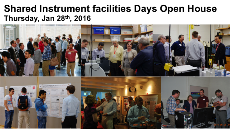
When: Thursday, January 28th, 9:00 am - 4pm
Location: Room 1025, Engineering Centers Building, UW Madison campus
1550 Engineering Drive, Madison 53706
Cost: FREE! but Registration required.
Labs presenting:
Materials Science Center
Soft Materials Lab
Wisconsin Center for Applied Microelectronics
Biochemistry Optical Core
Paul Bender Chemical Instrumentation Center
Student Posters - discussing instrument use in their research
Instruments highlights:
J.A. Woollam spectroscopic ellipsometers (UV, Vis, IR(up to 30.0 microns)
Hysitron TI 950 Tribo Indenter
Nikon N-STORM super resolution microscope
and more!
Questions? Please let us know:
Felix Lu, [email protected], (608) 262-6099
Erin Gill, [email protected], (608) 263-0612
|
|
UW Materials Science in the news
|
|
|
| The red abalone makes the lustrous but hard-as-nails nacre lining of its shell by changing the atomic structure of amorphous calcium carbonate to produce crystalline aragonite_ the mineral that is the basis of nacre. Also known as mother-of-pearl_ nacre has been worked by humans for millennia to make jewelry and fancy inlay for furniture and musical instruments. Image_ Pupa Gilbert |
Pearls have either been coveted or discarded without second thought. The importance applied to the object largely depends on culture. According to the
American Museum of Natural History, Polynesian children used pearls as marbles. However, many groups placed importance not on pearls, but their housing. After ingesting the mollusks, the leftover iridescent shells were used as decorative inlay for objects carved from wood, ivory and bone.
The composite responsible for the flashy coloring is nacre, or mother-of-pearl.
"An amorphous precursor to nacre formation has been suspected to exist, but has never been successfully identified, despite extensive attempts" write a team of researchers recently in the Journal of the American Chemical Society.
Now, those researchers have gained some insight into how this biomineral is formed at the atomic and nanometer scale, presenting the first observations of amorphous calcium carbonate to nacre formation.
Amorphous calcium carbonate minerals have been identified as the first phases of biominerals deposited by living organisms. "Sea urchin embryonic spicules were the first biominerals in which an amorphous precursor was discovered, followed by sea urchin spines and teeth, bone, tooth enamel and a variety of other biominerals," the researchers write.
"People have been trying to understand if nacre had an amorphous calcium carbonate precursor for a long time," said Pupa Gilbert, a physics professor at Univ. of Wisconsin-Madison and an expert on biomineral formation.
The team used the U.S. Dept. of Energy's Advanced Light Source, located at the Lawrence Berkeley National Laboratory, to observe the chemical transformation taking place when amorphous calcium carbonate transforms into aragonite, a mineral that manifests as nacre.
Read more:
http://www.rdmag.com/articles/2015/10/how-mother-pearl-forms?et_cid=4894451&et_rid=614174443&type=cta
|
|
|
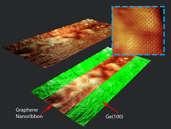
| Researchers at Argonne's Center for Nanoscale Materials have confirmed the growth of self-directed graphene nanoribbons on the surface of the semiconducting material germanium by researchers at the University of Wisconsin at Madison. |
By Justin H.S. Breaux * October 13, 2015
In a development that could revolutionize electronic ciruitry, a research team from the University of Wisconsin at Madison (UW) and the U.S. Department of Energy's Argonne National Laboratory has confirmed a new way to control the growth paths of graphene nanoribbons on the surface of a germainum crystal.
Germanium is a semiconductor, and this method provides a straightforward way to make semiconducting nanoscale circuits from graphene, a form of carbon only one atom thick.
The method was discovered by UW scientists and confirmed in tests at Argonne.
"Some researchers have wanted to make transistors out of carbon nanotubes, but the problem is that they grow in all sorts of directions," said Brian Kiraly of Argonne. "The innovation here is that you can grow these along circuit paths that works for your tech."
UW researchers used chemical vapor deposition to grow graphene nanoribbons on germanium crystals. This technique flows a mixture of methane, hydrogen, and argon gases into a tube furnace. At high temperatures, methane decomposes into carbon atoms that settle onto the germanium's surface to form a uniform graphene sheet. By adjusting the chamber's settings, the UW team was able to exert very precise control over the material.
"What we've discovered is that when graphene grows on germanium, it naturally forms nanoribbons with these very smooth, armchair edges," said
Michael Arnold, an associate professor of materials science and engineering at UW-Madison. "The widths can be very, very narrow, and the lengths of the ribbons can be very long, so all the desirable features we want in graphene nanoribbons are happening automatically with this technique."
Read more:
http://www.anl.gov/articles/one-direction-researchers-grow-nanocircuitry-semiconducting-graphene-nanoribbons?
http://www.forbes.com/sites/sujatakundu/2015/11/03/new-method-of-graphene-nanoribbon-production-shows-promise-for-energy-efficient-electronics/?utm_source=COE%20permstaff&utm_campaign=ab2e76df76-December_2015_News_Notes12_10_2015&utm_medium=email&utm_term=0_2d964b6256-ab2e76df76-278862025
|
Closely integrating both theory and experiments, a multidisciplinary team of researchers has discovered that reducing the size of certain electronic devices can cause them to become ferroelectric, or spontaneously polarized.
In addition to carving a path toward smaller and more convenient devices with increased storage capacity, this discovery will allow researchers to explore diverse nanoelectric functions in low-dimensional material systems.
In a paper published September 18, 2015, in the journal Science, a team led by University of Wisconsin-Madison engineer
Chang-Beom Eom described a phenomenon that completely overrides existing notions about ferroelectricity in nanoelectric devices.
"It's a breakthrough in science that overcomes conventional wisdom, which says that as anything gets smaller, properties start to fade and eventually disappear," says Eom, who is the Theodore H. Geballe Professor and Harvey D. Spangler Distinguished Professor of
materials science and engineering at UW-Madison. "But this actually shows that when we use a smaller scale, important properties begin to appear."
Eom and his collaborators worked with ultra-thin films made from the material strontium titanate-a perovskite dielectric material that is not ferroelectric. However, they found that they could align naturally existing polar nanoregions in the material in a specific way to provoke an increase in stable net ferroelectric polarization. They were able to do this without cooling the material-which is an important requirement for applications.
Read more:
http://www.engr.wisc.edu/news/archive/2015/Sept21.html
|
|
|
| The new type of glass developed by Juan de Pablo and his associates resembles this sample, which was produced at the Univ. of Wisconsin-Madison, in connection with a related project. Image: Prof. Mark Ediger/Univ. of Wisconsin |
Prof. Juan de Pablo's 20-year exploration of the unusual properties of glass began, oddly enough, with the microscopic animals known as water bears.
The creatures, which go by the more formal name of tardigrades, have a remarkable ability to withstand extreme environments of hot and cold, and even the vacuum of space. When de Pablo read about what happens when scientists dry out tardigrades, then revive them with water years later, his interest was piqued.
"When you remove the water, they very quickly coat themselves in large amounts of glassy molecules," says de Pablo, the Liew Family Professor in Molecular Engineering at the Univ. of Chicago. "That's how they stay in this state of suspended animation."
His passion to understand how glass forms in such exotic settings helped lead de Pablo and his fellow researchers to the unexpected discovery of a new type of glass.
This spring de Pablo and his collaborators at UChicago and the Univ. of Wisconsin-Madison published their findings in the Proceedings of the National Academy of Sciences. News of the breakthrough recently went viral online. A new paper bolsters the earlier glass research, which found indications of molecular order in a material thought to be entirely amorphous and random.
"These are intriguing materials. They have the structure of a liquid, and yet they're solids. They're found everywhere, and we still do not understand how this process of turning from a liquid into a solid occurs," says de Pablo.
Their results potentially offer a simple way to improve the efficiency of electronic devices such as light-emitting diodes, optical fibers, and solar cells. They also could have important theoretical implications for understanding the still surprisingly mysterious materials called glasses.
Read more:
http://www.uchicago.edu/features/microscopic_animals_inspire_innovative_glass_research/?
|
Directed by UW-Madison chemistry Professor
Robert Hamers, the center focuses on the molecular mechanisms by which nanoparticles interact with biological systems.
Nanotechnology involves the use of materials at the smallest scale, including the manipulation of individual atoms and molecules. Products that use nanoscale materials range from beer bottles and car wax to solar cells and electric and hybrid car batteries. If you read your books on a Kindle, a semiconducting material manufactured at the nanoscale underpins the high-resolution screen.
While there are already hundreds of products that use nanomaterials in various ways, much remains unknown about how these modern materials and the tiny particles they are composed of interact with the environment and living things.
"The purpose of the center is to explore how we can make sure these nanotechnologies come to fruition with little or no environmental impact," explains Hamers. "We're looking at nanoparticles in emerging technologies."
In addition to UW-Madison, scientists from UW-Milwaukee, the University of Minnesota, the University of Illinois, Northwestern University and the Pacific Northwest National Laboratory have been involved in the center's first phase of research. Joining the center for the next five-year phase are Tuskegee University, Johns Hopkins University, the University of Iowa, Augsburg College, Georgia Tech and the University of Maryland, Baltimore County.
Read more:
http://news.wisc.edu/23974?utm_source=iUW&utm_medium=email&utm_campaign=iUW2015-09-01
|
|
|
| Developed by UW-Madison electrical engineers_ this unique phototransistor is flexible_ yet faster and more responsive than any similar phototransistor in the world. Credit_ Jung-Hun Seo |
Inspired by mammals' eyes, University of Wisconsin-Madison electrical engineers have created the fastest, most responsive flexible silicon phototransistor ever made.
The innovative phototransistor could improve the performance of myriad products-ranging from digital cameras, night-vision goggles and smoke detectors to surveillance systems and satellites-that rely on electronic light sensors. Integrated into a digital camera lens, for example, it could reduce bulkiness and boost both the acquisition speed and quality of video or still photos.
Developed by UW-Madison collaborators Zhenqiang "Jack" Ma, professor of electrical and computer engineering, and research scientist Jung-Hun Seo, the high-performance phototransistor far and away exceeds all previous flexible phototransistor parameters, including sensitivity and response time.
The researchers published details of their advance this week in the journal Advanced Optical Materials.
Like human eyes, phototransistors essentially sense and collect light, then convert that light into an
electrical charge proportional to its intensity and wavelength. In the case of our eyes, the electrical impulses transmit the image to the brain. In a digital camera, that electrical charge becomes the long string of 1s and 0s that create the digital image.
While many phototransistors are fabricated on rigid surfaces, and therefore are flat, Ma and Seo's are flexible, meaning they more easily mimic the behavior of mammalian eyes.
"We actually can make the curve any shape we like to fit the optical system," Ma says. "Currently, there's no easy way to do that."
One important aspect of the success of the new phototransistors is the researchers' innovative "flip-transfer" fabrication method, in which their final step is to invert the finished phototransistor onto a plastic substrate. At that point, a reflective metal layer is on the bottom.
Read more:
http://news.wisc.edu/23974?utm_source=iUW&utm_medium=email&utm_campaign=iUW2015-09-01
|
|
|
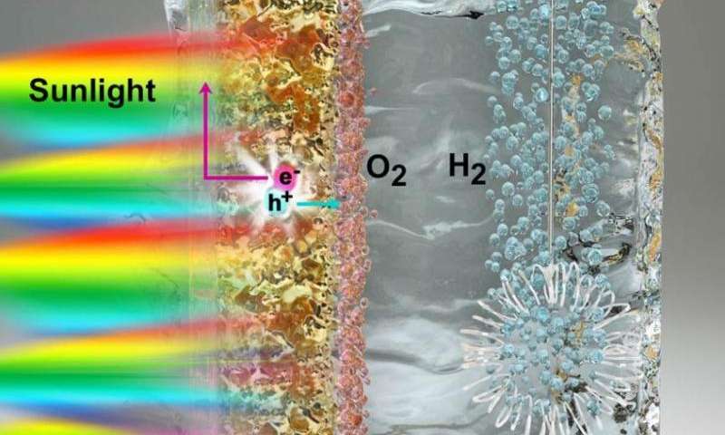
| Splitting water into hydrogen provides a means of harvesting the hydrogen for fuel. This image depicts the water-splitting process in a light-sensitive electrode material _BiVO4__ which UChicago and University of Wisconsin researchers investigated in an experimental and computational study. Credit_ Peter Allen Read more at_ http___phys.org_news_2015-10-concepts-emerge-inexpensive-fuel.html_jCp |
An inexpensive method for generating clean fuel is the modern-day equivalent of the philosopher's stone. One compelling idea is to use solar energy to split water into its constituent hydrogen and oxygen and then harvest the hydrogen for use as fuel. But splitting water efficiently turns out to be not so easy.
Now two scientists at the Institute for Molecular Engineering and the University of Wisconsin have made an important contribution to the effort, improving the efficiency of the key processes and offering new conceptual tools that can be applied more broadly in the quest to split water with sunlight. Their results appeared online Oct. 26 in Nature Communications.
In the research, Giulia Galli, the Liew Family Professor of Electronic Structure and Simulations at the IME,
|
|
| UW Madison Chemistry Professor Kyoung-Shin Choi |
and Kyoung-Shin Choi, a professor of chemistry at the University of Wisconsin, found a way to increase the efficiency with which an
electrode used for
splitting water absorbs solar photons-while at the same time improving the flow of
electrons from one electrode to another.
Simulations allowed them to understand what was happening at the atomic level. "Our study will encourage researchers in the field to develop ways to improve multiple processes using a single treatment," said Choi. "So it's not just about achieving higher efficiency, it's about providing a strategy for the field."
Read more:
http://phys.org/news/2015-10-concepts-emerge-inexpensive-fuel.html
|
|
|
| Tiny silicon nanowire towers make up dark regions of the flexible Fresnel zone lenses. Each individual lens resembles a bull_s-eye of alternating light and dark. Arrays of lenses formed within a flexible polymer bend and stretch into different configurations. Image_ Hongrui Jiang |
Drawing inspiration from an insect's multi-faceted eye, Univ. of Wisconsin-Madison engineers have created miniature lenses with vast range of vision.
Their new approach created the first-ever flexible Fresnel zone plate microlenses with a wide field of view-a development that could allow everything from surgical scopes to security cameras to capture a broader perspective at a fraction of the size required by conventional lenses.
Led by Hongrui Jiang, professor of electrical and computer engineering at UW-Madison, the researchers designed lenses no larger than the head of a pin and embedded them within flexible plastic. An array of the miniature lenses rolled into a cylinder can capture a panorama image covering a 170-degree field of view.
"We got the idea from compound eyes," says Jiang, whose work was published in Scientific Reports. "We
|
|
| UW Madison ECE Professor Hongrui Jiang |
know that multiple lenses on a domed structure give a large field of view."
And the researchers can freely reconfigure the shape of the lens array, because rather than relying on conventional optics for focusing, they used Fresnel zone plates.
Conventional lenses use refraction-the way light changes direction while passing through different substances (typically stiff, translucent ones, like glass)-to focus it on a single point. Named for 19th-century engineer Augustin-Jean Fresnel, the zone plates focus by diffraction-bending light as it passes the edge of a barrier.
Each of Jiang's half-millimeter diameter lenses resembles a series of ripples on water emanating out from the splash of a stone. In bull's-eye fashion, each concentric ring alternates between bright and dark. The distance between the rings determines the optical properties of the lens, and the researchers can tune those properties in a single lens by stretching and flexing it.
Previous attempts at creating Fresnel zone plate lenses have suffered from fuzzy vision.
Read more:
http://www.rdmag.com/news/2015/11/tiny-flexible-compound-lenses-magnify-large-fields-view?et_cid=4921570&et_rid=614174443&type=cta
|
|
|
Flats of the rapid-cycling Brassica plant are housed in a greenhouse of the Wisconsin Fast Plants Program in the Biotron Laboratory at the University of Wisconsin-Madison. The seeds from these plants are distributed to researchers around the world.
Photo: Bryce Richter
|
One of the most flexible and unique research facilities in North America is sitting in plain sight, but near anonymity, on the west side of the University of Wisconsin-Madison campus.
"When I tell people I work at
the Biotron, they say, 'Oh, I've walked by that building a million times, and I never knew what went on in there,' " explains its assistant director, Isabelle Girard. " 'It seems so secretive, with no windows.' But it's really easy to understand what we do here, whether you're a part of the university or not."
Here's the Biotron's big secret: It is whatever you want it to be (within terrestrial reason).
Built by the
National Science Foundation in the 1960s at 2115 Observatory Drive, the Biotron was designed to be able to simulate every climate on Earth except Antarctica. Scores of lab rooms spread across three floors can deliver temperatures from -20 degrees to 45 degrees Celsius (about -4 to 113 Fahrenheit), from 100 percent relative humidity down to nearly none, and light intensity from dark to half-strength daylight - which is more blinding than it sounds.
There are rooms tall enough for growing trees, and rooms isolated from sound and vibration. There are even hypobaric (low-pressure) chambers whose thin atmosphere has provided the simulated circumstances needed to test devices built to administer accurate doses of vaccines and drugs at high altitude.
That kind of flexibility has drawn in industrial clients from Harley Davidson to Parker Pen to Middleton-based Springs Window Fashions that subject their products to extremes and benchmark their performance in precisely monitored conditions. And it gives academic researchers the opportunity to design experiments that couldn't happen in conventional lab space - or without committing substantial time and money to one-off lab construction.
Read more:
http://news.wisc.edu/biotron-puts-any-environment-on-earth-within-researchers-reach/
|
Ceramic materials are ideal for a wide range of applications from jet engine components to intricate microelectromechanical parts. Unfortunately, because they cannot be cast or machined easily, ceramic parts are generally more difficult to process compared to polymers or metals. However, a new approach for producing ceramics using additive manufacturing overcomes the traditional limitations on ceramic processing.
3D Printing Ceramics
Ceramic parts are traditionally consolidated from powders by sintering. This inevitably leaves residual porosity in the parts, limiting their strength as well as their range of achievable final shapes.
The new approach utilizes a preceramic monomer resin which can be 3D-printed into parts of virtually any shape or size. Using a laser to raster the geometry of a part in the resin cures that portion of the resin into a polymer. Once cured, the resin is then fired to yield the final product: a high-strength, fully dense ceramic part.
|
|
|
| Stabilized flames of different metal powders burn with air_ compared to a methane-air flame. Credit_ Alternative Fuels Laboratory_McGill University |
Study points to metal powders as potential replacement for fossil fuels
Can you imagine a future where your car is fueled by iron powder instead of gasoline?
Metal powders, produced using clean primary energy sources, could provide a more viable long-term replacement for fossil fuels than other widely discussed alternatives, such as hydrogen, biofuels or batteries, according to a study in the Dec. 15 issue of the journal Applied Energy.
"Technologies to generate clean electricity - primarily solar and wind power - are being developed rapidly; but we can't use that electricity for many of the things that oil and gas are used for today, such as transportation and global energy trade," notes McGill University professor Jeffrey Bergthorson, lead author of the new study.
"Biofuels can be part of the solution, but won't be able to satisfy all the demand; hydrogen requires big, heavy fuel tanks and is explosive, and batteries are too bulky and don't store enough energy for many applications," says Bergthorson, a mechanical engineering professor and Associate Director of the Trottier Institute for Sustainability in Engineering and Design at McGill. "Using metal powders as recyclable fuels that store clean primary energy for later use is a very promising alternative solution."
Novel concept
The Applied Energy paper, co-authored by Bergthorson with five other McGill researchers and a European Space Agency scientist in the Netherlands, lays out a novel concept for using tiny metal particles - similar in size to fine flour or icing sugar - to power external-combustion engines.
|
|
|
| These are graphene flakes in the plastics graphene compound magnified 40.000 times CREDIT University of Luxembourg |
Physicists discover material for a more efficient energy storage
Predictions of physicists of the University of Luxembourg recently lead to the discovery of a material with special electric properties that engages the interest of plastics producing industry. Three years ago, physicists from Luxembourg had theoretically predicted the unusual characteristics of a particular composite material. These calculations could now be confirmed by experiment in cooperation with the "Centre de Recherche Paul Pascal" in Bordeaux, France, and resulted in the discovery of a so-called high-k-material, which might enable the production of better energy storage devices - the basis for smaller, faster and more efficient electronics.
The earlier calculations made by the team around Tanja Schilling, professor of physics at the University of Luxembourg, were at first rather bad news for the field of materials research: they indicated that certain compound materials made of polymers and flaky graphene, unlike those made of polymers and carbon nanotubes, did not increase the conductivity of the material to the degree that was generally expected until then. It was a surprising conclusion at the time which questioned the use of graphene in order to increase conductivity.
This prediction, however, now lead to a highly promising discovery: the effect that put the conductivity of the plastics-graphene-compound into question, causes it to have remarkable dielectric properties. This means that one can generate a strong electric field inside of it - the fundamental property for the production of efficient capacitors. These are tiny components that can store energy statically and occur in almost all electronic devices, where they act as voltage regulators or information storage, among other things. Computers, for example, contain billions of those.
|
|
|
|
By manipulating the structure of aluminum oxide_ a dielectric material_ researchers were able to improve its optical and mechanical properties. The key to the film_s performance is the highly ordered spacing of the pores_ which gives it a more mechanically robust structure without impairing the refractive index. You can see the structure here_ on the micrometer scale. Image_ Chih-Hao Chang
|
Dielectric film has refractive index close to air
Researchers from North Carolina State Univ. have developed a dielectric film that has optical and electrical properties similar to air, but is strong enough to be incorporated into electronic and photonic devices, making them both more efficient and more mechanically stable.
At issue is something called refractive index, which measures how much light bends when it moves through a substance. Air, for example, has a refractive index of 1, while water has a refractive index of 1.33-which is why a straw appears to bend when you put it in a glass of water.
Photonic devices require a high contrast between its component materials, with some components having a high refractive index and others have a low one. The higher the contrast between those materials, the more efficient the photonic device is, and the better it performs. Air has the lowest refractive index, but it isn't mechanically stable. And the lowest refractive index found in solid, naturally occurring materials is 1.39.
But now researchers have developed a film made of aluminum oxide that has a refractive index as low as 1.025 but that is mechanically stiff.
"By manipulating the structure of the aluminum oxide, which is dielectric, we've improved both its optical and mechanical properties," says Chih-Hao Chang, corresponding author of a paper on the work and an assistant professor of mechanical and aerospace engineering at NC State. Dielectrics are insulator materials that are used in an enormous array of consumer products. For example, every handheld device has hundreds of capacitors, which are dielectric components that can store and manage electric charge.
http://www.rdmag.com/news/2015/10/dielectric-film-has-refractive-index-close-air?et_cid=4874003&et_rid=614174443&location=top
|
Scientists in Japan have developed
an adhesive that starts out as powder but transforms into glue for hard-to-reach places when pressed. This represents a promising application for liquid marble technology.
Liquid marbles are millimetre-sized liquid droplets that when coated in a hydrophobic powder, lose their wetness. Pressure-sensitive adhesives (PSAs) are viscoelastic polymers that instantly stick to solid surfaces through van der Waals forces. They are used in tapes, labels, post-it notes, spray droplets and adhesives, but PSAs' sticky nature can make them difficult to handle. Combining these two technologies,
Syuji Fujii and his team at the Osaka Institute of Technology in Japan and co-workers at the Max-Planck Institute for Polymer Research in Germany have developed liquid marbles made up of soft poly(n-butyl acrylate) latex polymer particles that form a tacky polymer core coated with a hard hydrophobic calcium carbonate nanoparticle shell. Initially, the marbles show no adhesive properties but by applying shear stress - light contact pressure between finger and thumb for 1-30 seconds - the powder's nanoparticle layers rupture, allowing the soft inner polymer to ooze out, endowing the material with adhesive properties.
'Adhesion has been a crucial technology throughout all the ages and lands,' reflects Fujii. 'Whether building the Tower of Babel or fabricating smartphones, adhesion technology is absolutely essential. Technologies may come and go but adhesion is unaffected by changes in fashion.'
|

Steel is ubiquitous in our daily lives. We cook in stainless steel skillets, ride steel subway cars over steel rails to our offices in steel-framed building. Steel screws hold together broken bones, steel braces straighten crooked teeth, steel scalpels remove tumors. Most of the goods we consume are delivered by ships and trucks mostly built of steel.
While various grades of steel have been developed over the past 50 years, steel surfaces have remained largely unchanged-and unimproved. The steel of today is as prone as ever to the corrosive effects of water and salt and abrasive
materials such as sand. Steel surgical tools can still carry microorganisms that cause deadly infections.
Now, researchers at the Harvard John A. Paulson School of Engineering and Applied Sciences (SEAS) have demonstrated a way to make steel stronger, safer and more durable. Their new surface coating, made from rough nanoporous
tungsten oxide, is the most durable anti-fouling and anti-corrosive material to date, capable of repelling any kind of liquid even after sustaining intense structural abuse.
The new material joins the portfolio of other non-stick, anti-fouling materials developed in the lab of Joanna Aizenberg, the Amy Smith Berylson Professor of Materials Science and core faculty member of the Wyss Institute for Biologically Inspired Engineering at Harvard University. Aizenberg's team developed Slippery Liquid-Infused Porous Surfaces in 2011 and since then has demonstrated a broad range of applications for the super-slick coating, known as SLIPS. The new SLIPS-enhanced steel is described in Nature Communications.
|
|
|
| Students who gather their own data and make their own decisions in a simple pendulum experiment gain critical thinking skills that are useful in later physics courses, according to research at Stanford and the University of British Columbia. |
Introductory lab courses are ubiquitous in science education, but there has been little evidence of how or whether they contribute to learning. They are often seen as primarily "cookbook" exercises in which students simply follow instructions to confirm results given in their textbooks, while learning little.
In a
study published today in the Proceedings of the National Academy of Sciences, scientists from Stanford and the University of British Columbia show that guiding students to autonomous, iterative decision-making while carrying out common physics lab course experiments can significantly improve students' critical thinking skills.
In the multi-year, ongoing study, the researchers followed first-year students in co-author Douglas Bonn's introductory physics lab course at the University of British Columbia. They first established what students were, and were not, learning following the conventional instructional approach, and then systematically modified the instructions of some lab experiments to change how students think about data and their implications.
One of the first experiments the researchers tackled involved swinging a pendulum and using a stopwatch to time the period between two angles of amplitude. Students conducting the traditional experiment would collect the data, compare them to the equation in the textbook, chalk up any discrepancies to mistakes and move along.
In the modified course, the students were instructed to make decisions based on the comparison. First, what should they do to improve the quality of their data, and then, how could they better test or explain the comparison between data and the textbook result? These are basic steps in all scientific research.
Students chose improvements such as conducting more trials to reduce standard error, marking the floor to be more precise in measuring the angle, or simply putting the team member with the best trigger finger in charge of the stopwatch.
As their data improved, so did their understanding of the processes at work, as well as their confidence in their information and its ability to test predicted results.
Read more:
http://news.stanford.edu/news/2015/august/thinking-holmes-wieman-081715.html
|
|
Advanced Manufacturing and Related topics
|
|
|
| A schematic showing the formation of lithium hydroxide _LiOH_ on the graphene electrode on discharging a non-aqueous lithium-oxygen battery in the presence of the redox mediator_ lithium iodide_ and trace water. On charging_ the iodide is oxidized to iodine_ which helps to remove the LiOH and reform the bare graphene electrode. Credit_ Tao Liu_ Gabriella Bocchetti and Clare P. Grey Read more at_ http___phys.org_news_2015-10-path-ultimate-battery.html_jCp |
Scientists have developed a working laboratory demonstrator of a lithium-oxygen battery which has very high energy density, is more than 90% efficient, and, to date, can be recharged more than 2000 times, showing how several of the problems holding back the development of these devices could be solved.
Lithium-oxygen, or lithium-air, batteries have been touted as the 'ultimate'
battery due to their theoretical energy density, which is ten times that of a lithium-ion battery. Such a high energy density would be comparable to that of gasoline - and would enable an electric car with a battery that is a fifth the cost and a fifth the weight of those currently on the market to drive from London to Edinburgh on a single charge.
However, as is the case with other next-generation batteries, there are several practical challenges that need to be addressed before lithium-air batteries become a viable alternative to gasoline.
Now, researchers from the University of Cambridge have demonstrated how some of these obstacles may be overcome, and developed a lab-based demonstrator of a lithium-oxygen battery which has higher capacity, increased energy efficiency and improved stability over previous attempts.
Their demonstrator relies on a highly porous, 'fluffy' carbon electrode made from graphene (comprising one-atom-thick sheets of carbon atoms), and additives that alter the chemical reactions at work in the battery, making it more stable and more efficient. While the results, reported in the journal Science, are promising, the researchers caution that a practical lithium-air battery still remains at least a decade away.
Read more:
http://phys.org/news/2015-10-path-ultimate-battery.html
|
|
|
| On the right the cube represents the structure of lithium- and manganese- rich transition metal oxides. The models on the left show the structure from three different directions_ which correspond to the STEM images of the cube. Image_ Lawrence Berkeley National Laboratory |
Using complementary microscopy and spectroscopy techniques, researchers at Lawrence Berkeley National Laboratory (Berkeley Lab) say they have solved the structure of lithium- and manganese-rich transition metal oxides, a potentially game-changing battery material and the subject of intense debate in the decade since it was discovered.
Researchers have been divided into three schools of thought on the material's structure, but a team led by Alpesh Khushalchand Shukla and Colin Ophus spent nearly four years analyzing the material and concluded that the least popular theory is in fact the correct one. Their results were published online in Nature Communications. Other co-authors were Berkeley Lab scientists Guoying Chen and Hugues Duncan and SuperSTEM scientists Quentin Ramasse and Fredrik Hage.
This material is important because the battery capacity can potentially be doubled compared to the most commonly used Li-ion batteries today due to the extra lithium in the structure. "However, it doesn't come without problems, such as voltage fade, capacity fade, and DC resistance rise," said Shukla. "It is immensely important that we clearly understand the bulk and surface structure of the pristine material. We can't solve the problem unless we know the problem."
A viable battery with a marked increase in storage capacity would not only shake up the cell phone and laptop markets, it would also transform the market for electric vehicles (EVs). "The problem with the current lithium-ion batteries found in laptops and EVs now is that they have been pushed almost as far as they can go," said Ophus. "If we're going to ever double capacity, we need new chemistries."
Using state-of-the-art electron microscopy techniques at the National Center for Electron Microscopy (NCEM) at Berkeley Lab's Molecular Foundry and at SuperSTEM in Daresbury, U.K., the researchers imaged the material at atomic resolution. Because previous studies have been ambiguous about the structure, the researchers minimized ambiguity by looking at the material from different directions, or zone axes. "Misinterpretations from electron microscopy data are possible because individual 2-D projections do not give you the three-dimensional information needed to solve a structure," Shukla said. "So you need to look at the sample in as many directions as you can."
Read more:
http://www.rdmag.com/news/2015/10/battery-mystery-solved?et_cid=4910137&et_rid=614174443&type=cta
|
|
|
| An Impeller-based active mixer. Each fluid enters the mixing chamber through a separate inlet and is mixed in a narrow gap by an impeller rotating at a constant rate. Credit: Thomas Ober, Harvard SEAS/Wyss Institute |
3D printing is revolutionizing the production of lightweight structures, soft robots and flexible electronics, but the technology struggles with complex, multimaterial integration.
To print a flexible device, including the electronics, a 3D printer must be able to seamlessly transition from a flexible material that moves with your joints for wearable applications, to a rigid material that accommodates the electronic components. It would also need to be able to embed electrical circuitry using multiple inks of varying conductivity and resistivity, precisely switching between them. And, it would be ideal to do all of this without the stopping the printing process.
The ability to integrate disparate materials and properties within printed objects is the next frontier in 3D printing.
Towards this objective, Harvard researchers have designed new multimaterial printheads that mix and print concentrated viscoelastic inks that allow for the simultaneous control of composition and geometry during printing. Using active mixing and fast-switching nozzles, these novel printheads change material composition on the fly and could pave the way for entirely 3D-printed wearable devices, soft robots, and electronics.
The research was led by Jennifer A. Lewis, the Hansjörg Wyss Professor of Biologically Inspired Engineering at the Harvard John A. Paulson School of Engineering and Applied Sciences (SEAS) and a Core Faculty Member at the Wyss Institute for Biologically Inspired Engineering at Harvard. The work was published in the Proceedings of the National Academy of Sciences (PNAS).
Read more at:
http://phys.org/news/2015-09-lightweight-flexible-functional-materials.html#jCp
Read more:
http://phys.org/news/2015-09-lightweight-flexible-functional-materials.html
|
|
|
| The glass 3-D printing process. Image: Steven Keating |
The technology behind 3-D printing-which initially grew out of work at Massachusetts Institute of Technology (MIT)-has exploded in recent years to encompass a wide variety of materials, including plastics and metals. Simultaneously, the cost of 3-D printers has fallen sufficiently to make them household consumer items.
Now, a team of MIT researchers has opened up a new frontier in 3-D printing: the ability to print optically transparent glass objects.
The new system, described in the Journal of 3D Printing and Additive Manufacturing, was developed by Neri Oxman, an associate professor at the MIT Media Lab; Peter Houk, director of the MIT Glass Lab; MIT researchers John Klein and Michael Stern; and six others.
Other groups have attempted to 3-D print glass objects, but a major obstacle has been the extremely high temperature needed to melt the material. Some have used tiny particles of glass, melded together at a lower temperature in a technique called sintering. But such objects are structurally weak and optically cloudy, eliminating two of glass's most desirable attributes: strength and transparency.
The high-temperature system developed by the MIT team retains those properties, producing printed glass objects that are both strong and fully transparent to light. Like other 3-D printers now on the market, the device can print designs created in a computer-assisted design program, producing a finished product with little human intervention.
Read more:
http://www.rdmag.com/news/2015/09/printing-transparent-glass-3-d?et_cid=4812268&et_rid=614174443&type=cta
|
|
|
| The wobbling of the glass thread can produce different repeating patterns |
US researchers have developed what they call a "molten glass sewing machine" by combining 3D printing of glass with a mathematical model of how a liquid thread forms different types of loop.
When the nozzle releasing a stream of molten glass is raised above a certain level, that thread begins to wobble.
It traces out waves or loops - which the team found could be controlled by adjusting the speed of the nozzle.
Those shapes then become the building blocks for intricate, 3D objects.
Engineers at the Massachusetts Institute of Technology pioneered a method for glass 3D printing
in 2015. They then started to work with mathematician Pierre-Thomas Brun, who has
studied the fluid dynamics of liquid "ropes".
It all started with a collaboration between two labs at MIT, Dr Brun told the BBC - one specialising in
glass and the other in "
mediated matter".
Runny honey
"Normally when you 3D print, the nozzle is very close to the piece that you're printing - that's the conventional method. But what they started working with was having a large offset.
"And in that case, instead of having a thread that falls down and moves straight, you can create coil-like patterns like honey on toast."
That coiling process, as it happens, is exactly what Dr Brun studied during his PhD.
Read more:
http://www.bbc.com/news/science-environment-35171408
|
|
Photonic and Electronic Materials & Devices
|
|
|
| Illustration_ Peter Allen_Harvard SEAS |
One class of
metamaterials, with a refraction index of zero [pdf], was first created in 2013 and quickly caught the interest of scientists because of the materials' unique properties.
Such a material, when irradiated with light, behaves in a peculiar way, explains
Eric Mazur
, who leads a team of researchers investigating metamaterials at
Harvard University
in Cambridge, MA. For example, light directed at a planar slab can only pass when its incident angle is exactly 90 degrees. Says Mazur:
The light sets up a response in the material so that combined with the incident electromagnetic field the field in the material has the same phase throughout the material-not unlike the wheels of a carriage in a movie can appear at rest due to the interplay of the frequency of rotation and the frequency of the movie. This complete coherence in space, results in light with infinite wavelength and infinite phase velocity.
Since the phase of the light is the same in all of the metamaterial, it looks like the sinusoidal field has a wavelength that is streched to infinity and the phase propagates instantaneously. These two properties allow the light to be controlled in an unprecedented way in the very small space available on optical chips; it can travel through exteremely narrow channels or waveguides, and go around sharp corners without losing energy.
Now Mazur and his team at Harvard, working with researchers at
Peking University in Beijing,
report in the 19 October online edition of Nature Photonics the creation of an on-chip metamaterial with a refractive index of zero.
Read more:
http://spectrum.ieee.org/tech-talk/computing/hardware/zeroindex-metamaterials-open-new-possibilities-in-optical-chips?utm_campaign=Weekly%20Notification-%20IEEE%20Spectrum%20Tech%20Alert&utm_source=boomtrain&utm_medium=email&utm_term=555a972628fbca1d260da1ba&utm_content=Zero-Index%20Metamaterials%20Open%20New%20Possibilities%20for%20Optical%20Chips&bt_alias=eyJ1c2VySWQiOiIxYTJhZjY5ZS0zMDRjLTRhYTQtOWM4ZC1mN2ExMzc1OTk0NzQifQ%3D%3D
|
A revolutionary breakthrough is underway at Dartmouth's Thayer School of Engineering, an innovation that may usher in the next generation of light sensing technology with potential applications in scientific research and cellphone photography.
Thayer professor Eric Fossum-the engineer and physicist who invented the
CMOS image sensor used in nearly all cellphone and digital cameras, webcams, medical imaging and other
applications-joined with Thayer PhD candidate Jiaju Ma in developing pixels for the new
Quanta Image Sensor (QIS).
The professor and student, who have worked on the project for more than three years, are co-inventors of the new pixel and co-authors of a paper on their invention in
IEEE Electron Devices Letters.
Their new sensor has the capability to significantly enhance low-light sensitivity. This is particularly important in applications such as "security cameras, astronomy, or life science imaging (like seeing how cells react under a microscope), where there's only just a few
photons," says Fossum.
"Light consists of photons, little bullets of light that activate our neurons and make us see light," says Fossum. "The photons go into the semiconductor [the
sensor chip] and break the chemical bonds between silicon atoms and, when they break the bond, an electron is released. Almost every photon that comes in, makes one electron free inside the silicon crystal. The brighter the light, the more electrons are released."
Fossum says that one of the several challenges in the QIS is to count how many electrons are set free by photons and thus effectively count photons. This is particularly important in very low light applications, such as in
life science microscopy, photography, or even possibly quantum cryptography and the Internet of Things. "When we build an image sensor, we build a chip that is also sensitive to these photons. We were able to build a new kind of pixel with a sensitivity so high we could see one electron above all the background noise."
Read more at:
http://phys.org/news/2015-09-breakthrough-photography.html#jCp
Read more:
http://phys.org/news/2015-09-breakthrough-photography.html
|
|
|
| The circularly polarized light detector on a chip, on the left, performs the same function as the conventional, optically based detector on the right. Credit: Anne Rayner, Vanderbilt University |
Invention of the first integrated circularly polarized light detector on a silicon chip opens the door for development of small, portable sensors that could expand the use of polarized light for drug screening, surveillance, optical communications and quantum computing, among other potential applications.
The new detector was developed by a team of Vanderbilt University engineers directed by Assistant Professor of Mechanical Engineering Jason Valentine working with researchers at Ohio University. The work is described in an article published on Sept. 22 in the online journal Nature Communications.
"Although it is largely invisible to human vision, the polarization state of light can provide a lot of valuable information," said Valentine. "However, the traditional way of detecting it requires several optical elements that are quite bulky and difficult to miniaturize. We have managed to get around this limitation by the use of 'metamaterials' - materials engineered to have properties that are not found in nature."
Polarized light comes in two basic forms: linear and circular. In a ray of unpolarized light, the electrical fields of individual photons are oriented in random directions. In linearly polarized light the fields of all the photons lie in the same plane. In circularly polarized light (CPL), the fields lie in a plane that continuously rotates through 360 degrees. As a result there are two types of circularly polarized light, right-handed and left-handed.
Read more:
http://phys.org/news/2015-09-circularly-polarized-detector-silicon-chip.html
|
Flexible glass: current status, outlook and challenges
Flexible glass is a significant technical achievement, yet IDTechEx Research believes that it will not be the solution of choice for encapsulation of flexible electronics in the short to medium term, for multiple reasons.
In spite of the marketing spin given by the manufacturers, glass is inherently a fragile material and requires specialized handling and processing. While plastic materials can also be damaged, there is an important difference between the two: damage of barriers on plastic can lead to the failure of a specific part, however, shattering of glass, even if protective sheets are used, leads to particle contamination on the defect line able to affect multiple parts.
Inherent fragility of flexible glass makes sheet edges critical. All suppliers propose protective tabs to reduce the problem. However, any other particle on the processing equipment could also become a focal point of stress and lead to shattering of the glass sheet or web.
A strong point of traditional glass encapsulation (especially for top emission devices) has been its ability to form truly hermetic
packaging by using glass frit and laser sealing. This advantage may not be transferable to flexible glass where glass-to-glass sealing may be very problematic and difficult because points of stress and relative twisting of the two sheets must be avoided in the laser firing of the frit. It may be that flexible glass has to be used in combination with adhesives (and desiccants).
Flexibility is another issue. Although glass is very flexible if flexed along a well-defined axis, it can be poor at tolerating any stress out of axis, so much so that twisting the sheet may lead to fracture. This is true with or without protective film applied to the glass. Extreme flexibility (r< 2-3 mm) may also be a problem. Data that has been shown would put the flexibility limit around r= 2.5 cm. Consequently, flexible glass as an encapsulant superstrate or substrate may be good for conformal applications, but for truly flexible applications there seem to be several challenges to be overcome.
Flexible glass makers are also waiting for equipment providers to make appropriate equipment to handle the flexible glass in manufacturing, another bottle neck.
Future opportunities for flexible glass
The thermal stability of flexible glass makes it the best choice as substrate for back-planes of high-resolution high-end large
displays. Glass enables improved resolution and good registration between layers during processing compared to plastic substrates like PET, PEN, and PI. However, IDTechEx analysts and other affiliate experts have only seen results with metal oxide backplanes only so far (Tprocess < 350 C), none with LTPS backplanes (Tprocess < 450 C). If processability up to 450C is indeed possible, flexible glass would be a very good choice as a substrate for flexible
AMOLED TV. Those devices are bottom emission (BE) AMOLED, normally have a metal foil as back encapsulant, a higher cost tolerance. Regarding R2R processing of flexible glass, it has demonstrated possible. Manufacturing by R2R will require specialized tools not differently than fabrication of barrier in R2R.
Read more:
http://electroiq.com/blog/2015/08/status-of-flexible-encapsulation-to-enable-flexible-electronics/
|
|
Microstructured Thin FIlms and Coatings
|
|
|
| Fatigue-free flexible transparent electrode for stretchable and bendable electronics. Credit: University of Houston |
Researchers have discovered a new stretchable, transparent conductor that can be folded or stretched and released, resulting in a large curvature or a significant strain, at least 10,000 times without showing signs of fatigue.
This is a crucial step in creating a new generation of foldable electronics - think a flat-screen television that can be rolled up for easy portability - and implantable medical devices. The work, published Monday in the Proceedings of the National Academy of Sciences, pairs gold nanomesh with a stretchable substrate made with polydimethylsiloxane, or PDMS.
The substrate is stretched before the gold nanomesh is placed on it - a process known as "prestretching" - and the material showed no sign of fatigue when cyclically stretched to a strain of more than 50 percent.
Fatigue is a common problem for researchers trying to develop a flexible,
transparent conductor, making many
materials that have good electrical conductivity, flexibility and transparency - all three are needed for foldable electronics - wear out too quickly to be practical, said Zhifeng Ren, a physicist at the University of Houston and principal investigator at the Texas Center for Superconductivity, who was the lead author for the paper.
The new material, produced by grain boundary lithography, solves that problem, he said.
Read more:
http://phys.org/news/2015-09-fatigue-free-stretchable-conductor.html
|
|
|
| Schematic showing a new engineered surface that can repel liquids in any state of wetness. Image: Xiaming Dai, Chujun Zeng and Tak-Sing Wong/Penn State |
The leaves of the lotus flower, and other natural surfaces that repel water and dirt, have been the model for many types of engineered liquid-repelling surfaces. As slippery as these surfaces are, however, tiny water droplets still stick to them. Now, Penn State Univ. researchers have developed nano/micro-textured, highly slippery surfaces able to outperform these naturally inspired coatings, particularly when the water is a vapor or tiny droplets.
Enhancing the mobility of liquid droplets on rough surfaces could improve condensation heat transfer for power-plant heat exchangers, create more efficient water harvesting in arid regions, and prevent icing and frosting on aircraft wings.
"This represents a fundamentally new concept in engineered surfaces," said Tak-Sing Wong, assistant professor of mechanical engineering and a faculty member in the Penn State Materials Research Institute. "Our surfaces combine the unique surface architectures of lotus leaves and pitcher plants in such a way that these surfaces possess both high surface area and a slippery interface to enhance droplet collection and mobility. Mobility of liquid droplets on rough surfaces is highly dependent on how the liquid wets the surface. We have demonstrated for the first time experimentally that liquid droplets can be highly mobile when in the Wenzel state."
Liquid droplets on rough surfaces come in one of two states: Cassie, in which the liquid partially floats on a layer of air or gas, and Wenzel, in which the droplets are in full contact with the surface, trapping or pinning them. The two states are named for the physicists who first described them. While the Wenzel equation was published in 1936 in a highly cited paper, it has been extremely challenging to verify the equation experimentally.
"Through careful, systematic analysis, we found that the Wenzel equation does not apply for highly wetting liquids," said Birgitt Boschitsch Stogin, graduate student in Wong's group and co-author of "Slippery Wenzel State," published online in ACS Nano.
|
Bubble, bubble ... boiling on the double
New analysis of textured surfaces could lead to more efficient, and less dangerous, power plants.
|
|
| Postdoc Navdeep Singh Dhillon (pictured) studies the fundamental physical mechanisms that dictate the boiling crisis phenomenon. At right is a rig for measuring the critical heat flux (CHF) of thermally saturated water boiling on thin textured substrates, which allows researchers to visualize bubbles and measure real-time spatial substrate temperatures using infrared imaging. Photo: Jose-Luis Olivares/MIT |
The boiling of water is at the heart of many industrial processes, from the operation of electric power plants to chemical processing and desalination. But the details of what happens on a hot surface as water boils have been poorly understood, so unexpected hotspots can sometimes melt expensive equipment and disable plants.
Now researchers at MIT have developed an understanding of what causes this extreme heating - which occurs when a value known as the critical heat flux (CHF) is exceeded - and how to prevent it. The new insights could make it possible to operate power plants at higher temperatures and thus significantly higher overall efficiency, they say.
The findings are reported this week in the journal Nature Communications, in a paper co-authored by mechanical engineering postdoc Navdeep Singh Dhillon, professor of nuclear science and engineering Jacopo Buongiorno, and associate professor of mechanical engineering Kripa Varanasi.
"Roughly 85 percent of the worldwide installed base of electricity relies on steam power generators, and in the U.S. it's 90 percent," Varanasi says. "If you're able to improve the boiling process that produces this steam, you can improve the overall power plant efficiency."
The bubbles of vapor that characterize boiling, familiar to anyone who has ever boiled water on a stove, turn out to limit energy efficiency. That's because gas - whether it's air or water vapor - is highly insulating, whereas water is a good absorber of heat. So on a hot surface, the more area that is covered with bubbles, the less efficient the transfer of heat energy becomes.
If those bubbles persist too long at a given spot, it can significantly increase the temperature of the metal underneath, since heat is not transferred away fast enough, Varanasi says - and can potentially melt part of the metal.
Read more:
http://www.rdmag.com/news/2015/08/engineered-surface-unsticks-sticky-water-droplets?et_cid=4784480&et_rid=614174443&type=cta
|
|
Characterization of Advanced Materials
|
|
|
| In complex alloys_ chemical disorder results from a greater variety of elements than found in traditional alloys. Traces here indicate electronic states in a complex alloy_ smeared traces reduced electrical and thermal conductivity. Image_ Oak Ridge National Laboratory_ U.S. DOE_G. Malcolm Stocks |
Designing alloys to withstand extreme environments is a fundamental challenge for materials scientists. Energy from radiation can create imperfections in alloys, so researchers in an Energy Frontier Research Center led by the U.S. Dept. of Energy (DOE)'s Oak Ridge National Laboratory (ORNL) are investigating ways to design structural materials that develop fewer, smaller flaws under irradiation. The key, they report in Nature Communications, is exploiting the complexity that is present when alloys are made with equal amounts of up to four different metallic elements.
"Chemical complexity gives us a way to modify paths for energy dissipation and defect evolution," said first author Yanwen Zhang, who directs an Energy Frontier Research Center, called "Energy Dissipation to Defect Evolution," or "EDDE," funded by the DOE Office of Science. The growing center is nearly 15 months old and brings together more than two dozen researchers with experimental and modeling expertise. EDDE has partners at Oak Ridge, Los Alamos and Lawrence Livermore national laboratories and the universities of Michigan, Wisconsin-Madison and Tennessee-Knoxville.
Radiation can harm spacecraft, nuclear power plants and high-energy accelerators. Nuclear reactions produce energetic particles-ions and neutrons-that can damage materials as their energy disperses, causing the formation of flaws that evolve over time. Advanced structural materials that can withstand radiation are a critical national need for nuclear reactor applications. Today, nuclear reactors provide one-fifth of U.S. electricity. Next-generation reactors will be expected to serve over longer lifetimes and withstand higher irradiation levels.
In a reactor, thousands of atoms can be set in motion by one energetic particle that displaces them from sites in a crystal lattice. While most of the displaced atoms return to lattice sites as the energy is dissipated, some do not. Irradiation can damage structural materials made of well-ordered atoms packed in a lattice--even obliterating its crystallinity. Existing knowledge of radiation effects on structural materials is mostly about reactor-core components. Over the life of a typical light water reactor, all atoms in the structural components can be displaced on average 20 times, and accumulated damage may threaten material performance. To prepare for new reactor concepts, scientists will have to design next-generation nuclear materials to withstand atoms displaced more than 200 times-a true "grand challenge."
|
The ductility of magnesium explained
New analysis of textured surfaces could lead to more efficient, and less dangerous, power plants.
Zhaoxuan Wu and William Curtin of the Laboratory for Multiscale Mechanics Modeling (LAMMM) have solved the 40-year-old scientific riddle of the low ductility magnesium.
Magnesium is the lightest metal found on earth; it is four times lighter than steel and a third lighter than aluminum. It is also abundantly available, being the eight most common element in the earth's crust. These features should make it the ideal material for all kinds of uses, particularly in the automotive industry where fuel efficiency is greatly improved by reduced vehicle weight. However, the use of this metal remains marginal. "Magnesium has low ductility, that is, it cannot be stretched very much before it breaks. It also shows unusual behavior, such as a regime of increasing strength with increasing temperature, which is the opposite of most metals", said Prof. Curtin. The Director of the Institute of Mechanical Engineering and his collaborator Zhaoxuan Wu, a long-term visitor in LAMMM from the Institute for High Performance Computing in Singapore, were able to identify the atomistic origins of Magnesium's low ductility and unusual behavior.
This breakthrough, published in the journal Nature, could open the way to many applications of this lightweight metal.
Simulations to explain 40 years of experiments
Solving this mystery had an interesting history: long struggles, tangential advances, a new collaboration, and a "Eureka" moment. "I worked for 7 years on magnesium", says Curtin. "We had some accomplishments, but not on the most crucial issues, and I was about to give up, having exhausted what I thought we could do. But then Wu came from Singapore and brought renewed energy, an array of necessary technical skills, and exceptional motivation". Fast forward two years and the mystery is solved: they managed to establish a picture that unified decades of experimentation.
|
|
|
| In addition to the study_s senior author Gary Siuzdak_ authors included _left to right_ Michael Kurczy_ Mingliang Fang and H. Paul Benton of TSRI_s Scripps Center for Metabolomics. Credit_ The Scripps Research Institute. |
A new study led by scientists at The Scripps Research Institute (TSRI) shows that a technology used in thousands of laboratories, called gas chromatography mass spectrometry (GC-MS), fundamentally alters the samples it analyzes.
"We found that even relatively low temperatures used in GC-MS can have a detrimental effect on small molecule analysis," said study senior author Gary Siuzdak, senior director of TSRI's Scripps Center for Metabolomics and professor of chemistry, molecular and computational biology.
Using new capabilities within XCMS, a data analysis platform developed in the Siuzdak lab, the researchers observed small molecules transforming-and even disappearing-during an experiment meant to mimic the GC-MS process, throwing into question the nature of the data being generated by GC-MS.
The study was published online ahead of print on October 4 in the journalAnalytical Chemistry.
A Closer Look at GC-MS
For more than 50 years, chemists and biologists have used GC-MS to identify and measure concentrations of small molecules. When a sample is injected in a GC-MS system, it is heated and vaporized. The vapor travels through a gas chromatography column and the molecules separate, allowing the mass spectrometer to measure the individual molecules in the sample. Today, GC-MS is widely used in thousands of laboratories for tasks such as chemical analysis, disease diagnosis, environmental monitoring and even forensic investigations.
The new experiments were initiated when Siuzdak was preparing a short course for students at the American Society for Mass Spectrometry annual meeting. The question arose of how heat from the GC-MS vaporization process could affect results, so Siuzdak and TSRI Research Associate Mingliang Fang ran a set of experiments to compare how small molecules responded to thermal stress.
|
Yale Univ. scientists may have cracked a part of the chemical code for one of the most basic, yet mysterious, processes in the natural world-nature's ability to transform nitrogen from the air into usable nitrogen compounds.
The process is called nitrogen fixation, and it occurs in microorganisms on the roots of plants. This is how nature makes its own fertilizers to feed plants, which feed us.
The enzyme responsible for natural nitrogen fixation is called nitrogenase. Yale chemistry professor Patrick Holland and his team designed a new chemical compound with key properties that help to explain nitrogenase. The findings are described in Nature.
"Nitrogenase reacts with nitrogen at a cluster of iron and sulfur atoms, which is strange because other iron-sulfur compounds typically don't react with nitrogen, either in other enzymes or in the thousands of known iron-sulfur compounds synthesized by chemists," Holland said.
Read more:
http://news.mit.edu/2015/inexpensive-new-catalysts-fine-tuned-0916?
|
|
|
A new carbon-based catalyst can bond to the edges of two-dimensional sheets of graphene.
Courtesy of the researchers |
Material could replace precious metals and produce precisely controlled electrochemical reactivity.
Researchers at MIT and Lawrence Berkeley National Laboratory have developed a new type of catalyst that can be tuned to promote desired chemical reactions, potentially enabling the replacement of expensive and rare metals in fuel cells.
The new catalyst is carbon-based, made of graphite with additional compounds bonded to the edges of two-dimensional sheets of graphene that make up the material. By adjusting the composition and amounts of these added compounds, the characteristics of the catalyst can be adjusted to favor specific chemical reactions.
The new catalytic material is described in a paper published in JACS, the Journal of the American Chemical Society, by MIT assistant professor of chemistry Yogesh Surendranath and three collaborators.
Catalysts enhance the rate of a chemical reaction but are not consumed in the process. As a result, the repeated action of very small amounts of a catalyst can have large and long-lasting effects.
There are two basic types of electrocatalysts, which are crucial for enabling reactions in devices such as fuel cells or electrolyzers. Molecular electrocatalysts have the advantage of being relatively easy to tune by chemical treatment, so their reactivity and selectivity match the desired application; heterogeneous electrocatalysts, which are much more durable and easy to process into a device, tend to lack that ability for precise control.
"What we wanted to do was to figure out a way to bridge those two worlds," Surendranath explains. His team was able to accomplish that by taking graphite and finding a way to chemically modify its surface to give it the desired tunability.
The basic material used is pure carbon, which is "the universal electrode material" in batteries and fuel cells, Surendranath says. By finding a way to make this material tunable in the same ways as molecular catalysts, the researchers are providing an opening to a new approach to the design of such materials, which are also a key part of many chemical manufacturing processes.
Read more:
http://news.mit.edu/2015/inexpensive-new-catalysts-fine-tuned-0916?
|
|
Biomaterials and Biotechnology
|
|
|
| A type of yeast called Saccharomyces cerevisiae, makes a "small but significant" contribution to a wine's flavour and taste, scientists report |
Being a winemaker is a specialised calling, requiring intimate knowledge of soil composition, seasons and weather, chemistry, flavour, even marketing and sales.
Yet the distinctive bouquet and flavour of a Chablis or chardonnay could not be achieved without the input of a brainless,
single-celled organism, said a study Thursday.
The previously overlooked vintner, a type of yeast called Saccharomyces cerevisiae, makes a "small but significant" contribution to a wine's flavour and taste, scientists reported in the journal Scientific Reports.
This makes the fungus a key to that enigmatic wine concept "terroir"-everything from the soil, topography, climate and agricultural processes that go into producing your favourite Bordeaux.
"I was surprised that we detected any signal at all from these geographically different yeast populations in the aroma profile of the wine-I thought we would not," co-author Matthew Goddard of the University of Lincoln in England told AFP.
"The signal is small, but detectable," he said by email.
Geographic differences in wines were previously ascribed mainly to plant genetics, local soil and climate, and farming methods.
Read more:
http://phys.org/news/2015-09-wine-darkest-secret-revealed-.html
|
|
|
| Nanoporous gold is like a sponge of tiny pores. It could be used to make new devices to detect pathogens. Image: Erkin Şeker , UC Davis |
By Jocelyn Anderson
Sponge-like nanoporous gold could be key to new devices to detect disease-causing agents in humans and plants, according to UC Davis researchers.
In two recent papers in Analytical Chemistry (
here &
here), a group from the UC Davis
Department of Electrical and Computer Engineering demonstrated that they could detect nucleic acids using nanoporous gold, a novel sensor coating material, in mixtures of other biomolecules that would gum up most detectors. This method enables sensitive detection of DNA in complex biological samples, such as serum from whole blood.
"Nanoporous gold can be imagined as a porous metal sponge with pore sizes that are a thousand times smaller than the diameter of a human hair," said
Erkin Şeker, assistant professor of electrical and computer engineering at UC Davis and the senior author on the papers. "What happens is the debris in biological samples, such as proteins, is too large to go through those pores, but the fiber-like nucleic acids that we want to detect can actually fit through them. It's almost like a natural sieve."
Rapid and sensitive detection of nucleic acids plays a crucial role in early identification of pathogenic microbes and disease biomarkers. Current sensor approaches usually require nucleic acid purification that relies on multiple steps and specialized laboratory equipment, which limit the sensors' use in the field. The researchers' method reduces the need for purification.
"So now we hope to have largely eliminated the need for extensive sample clean-up, which makes the process conducive to use in the field," Şeker said.
The result is a faster and more efficient process that can be applied in many settings.
The researchers hope the technology can be translated into the development of miniature point-of-care diagnostic platforms for agricultural and clinical applications.
"The applications of the sensor are quite broad ranging from detection of plant pathogens to disease biomarkers," said Şeker.
For example, in agriculture, scientists could detect whether a certain pathogen exists on a plant without seeing any symptoms. And in sepsis cases in humans, doctors might determine bacterial contamination much more quickly than at present, preventing any unnecessary treatments.
Read more:
http://blogs.ucdavis.edu/egghead/2015/09/04/nanoporous-gold-sponge-makes-pathogen-detector/?
|
|
|
| Liquid gold being poured into a cast at Gold Reef City in Johannesburg, South Africa. Processing gold ore involves the use of cyanide, resulting in contaminated wastewater that needs to be remediated. In this study, researchers conducted metagenomic analyses to identify microbes that could help with the bioremediation process. Image: Dan Brown |
Researchers conducted analyses of microbial communities in laboratory-scale bioreactors breaking down contaminated wastewater from gold ore processing.
In this "first application of genome-resolved metagenomics" to characterize bioreactors involved in gold ore processing, the data reveal how the bioreactors utilize available nutrients in wastewater and allow researchers to observe which microbes dominate the communities, which will help improve microbial-based remediation strategies.
The Emerging Technologies Opportunity Program (ETOP) was launched in 2013 by the U.S. Dept. of Energy Joint Genome Institute (DOE JGI), a DOE Office of Science User Facility at Lawrence Berkeley National Laboratory. The Program aims to bring new technologies developed at other institutions into the DOE JGI, making them available to its users for energy and environment applications. A half a dozen proposals were approved during the Program's first year.
Among the projects approved in the inaugural ETOP call was one from metagenomics pioneer Jill Banfield at the Univ. of California, Berkeley. Banfield proposed building and characterizing a pipeline that would allow researchers to isolate and study both near-complete and complete microbial genomes from environmental samples. One of the results from this project was published in Environmental Microbiology.
Read more:
http://www.rdmag.com/news/2015/09/how-microbes-break-down-wastewater-contaminants?et_cid=4815935&et_rid=614174443&type=cta
|

If you used any instruments in the Materials Science Center, Soft Materials Laboratory, or the Wisconsin Center for Applied Microelectronics, please remember to acknowledge MRSEC funded instruments and facilities in any publications (DMR-1121288). This will serve as a metric for how often MRSEC funded instruments are used and will help continue MRSEC support in future years. Thanks! If you have any questions, please contact
Felix Lu
.
|
|
|

The Soft Materials Lab
The Soft Materials Lab, housed in the basement of Engineering Hall, has a wide spectrum of instruments for characterizing soft materials. The lab is managed by
Anna Kiyanova who is available to answer all of your characterization questions. Some of the instrumentation in the SML is listed below:
Gel Permeation Chromatography (GPC)
Dynamic Scanning Calorimetry (DSC)
Thermo-Gravimetric Analyzer (TGA)
Dynamical Mechanical Analyzer (DMA)
Rheometer
FTIR, PM-IRRAS, Fast Mapping Raman, Spin coater, Environmental SEM, Filmetrics F20 Reflectometer, Oxygen Plasma Asher, Contact Angle imager, atmospheric & vacuum ovens
Contact:
Anna Kiyanova
[email protected]
(608) 263-1735
|
The Materials Science Center (MSC)
The Materials Science Center has a wide spectrum of electron, optical and physical charaterization instruments, some of which are listed below. The MSC is fully staffed with highly experienced instrument expertise to help you with your sample characterization and data interpretation.
FE-SEMS with EDS
(S)TEMs with EDS/EELS & Cryo Capable
Atom Probe
XPS with Cluster Gun
AFM/BioAFM
Laser Scanning Confocal Microscope
Raman Microscope with multiple excitation sources
FTIR
ZYGO optical Profilometer
Fluorimeter
Tabletop SEM
UV-VIS spectrometer
Nano-Indenter
FIB
Sample Preparation facilities
sputter coaters/ion mills
XRDs
Contact:
Dr. Jerry Hunter
[email protected]
(608) 263-1073
|
The WCAM is a full spectrum micro/nano fabrication facility for processing and integrating devices in Silicon, III-V, group four, glass, plastic, materials. On site, fully-qualified and highly experienced staff are available to help you with your process development and answer questions. Processing capabilities include:
Photo/nanoimprint Lithography
wet/dry etching
metal /dielectric deposition
dielectric film growth
MEMS processing (critical point drying, wafer bonding and alignment, etc.)
packaging (wire bonding, die attach, dicing, curing)
Contact:
Dan Christensen
[email protected]
(608) 262-6877
|

Wisconsin GEO-Science materials characterization facility
The materials characterization facility in the Geology dept has some complementary instrumentation along with materials experts to help you with your charaterization and sample prep challenges! A partial list of instruments is listed below:
Electron Microprobe Analysis
SEM
XRD (with Cobalt source)
SIMS Lab
and many more!
Contact:
Dr. John Fournelle
Dept of Geology & Geophysics
University of Wisconsin-Madison
1215 W. Dayton St
Madison, WI 53706
(608) 262-7964 (office) 265-4798 (lab) 262-0693 (fax)
johnf*at*geology.wisc.edu
|

Science Cafes
What is a science café?
Science cafés are live grassroots events held in casual settings like coffeehouses and pubs that are open to everyone, organized locally and feature an engaging conversation with a scientist on a particular topic. Science cafés have been held in communities across the globe for years.
To learn more, visit sciencecafes.org
Who should attend?
Everyone! S
cience cafés are free and open to the public.
No prior scientific knowledge is needed, so anybody can participate.
What would I do at a science café?
Science cafés start with a presentation by a scientist or group of scientists about the evening's topic. Then the conversation about the topic begins.
A science café is not a formal lecture-audience members are encouraged to ask questions and participate in the discussion.
|
|
Student tour groups of your facility
|
Industrial facilities tours?
Are you interested in showing off your facility to interested student groups? Do you want to increase exposure of what your company does to encourage higher application rates and get student interns? Hosting a tour might be a good start! Please contact
Felix Lu or
Erin Gill to initiate this!
|
|
Using our campus facilities
|
|
The Practical Side of Things
|
One of the more common manufacturing methods has technicians making structured 3D semiconductors by first growing a crystal, then slicing and polishing it into a thin wafer, known as the substrate. Layers of crystals are grown on the substrate's surface and shot with ions to fill gaps in the 3D matrix of the semiconductor. This creates the p- and n-regions.
It has proven more cost-effective from a fabrication standpoint, since thousands of LEDs are made on a single wafer. For example, a 2-in. diameter wafer can yield up to 6,000 LEDs. However, producing a single LED chip from a wafer requires a specialized cutting process, which inevitably reduces the overall yield. Thus, to lower the price of LEDs and semiconductors, a better method is needed to separate them.
Read more!
http://machinedesign.com/embedded/abcs-leds
|
|
|
| Optical adhesives provide the strength needed to withstand extreme mechanical stress without interfering with optical transmission across a wide range of wavelengths. |
Optical System Design:
Polymeric systems bring
clarity to optical
applications
Optical-grade epoxies, silicones,and
ultraviolet (UV)-curable compounds offer engineers great versatility for bonding, sealing, coating, and encapsulation applications. These systems
adhere well to diverse substrates, and offer excellent temperature resistance, stress
relief, and protection from moisture and other corrosive elements. These materials play
an integral role not only in conventional fiber optics and optoelectronics systems, but also in various specialty medical, military, and aerospace devices.
Manufacturers can find both optically clear and optically opaque polymer systems that can tightly bond optical components built from materials that include polycarbonate, acrylic, quartz, glass, and fused silica. While opaque adhesives prevent any optical leakage, clear adhesives exhibit very flat transmission curves across a wide spectrum, providing an optically clear medium with a spectral transmission that extends from UV wavelengths as low as 250 nm through visible and infrared wavelengths of 2500 nm or even higher
Read more!
http://www.laserfocusworld.com/articles/print/volume-51/issue-09/features/optical-system-design-polymeric-systems-bring-clarity-to-optical-applications.html?cmpid=EnlLFWSeptember222015&eid=296499394&bid=1182567
|
Engineering majors enjoy some of the highest starting salaries in today's economy. In 2014, the top three engineering majors in terms of starting salary were petroleum, electrical, and computer engineering, according to the Bureau of Labor Statistics. But what is the key to getting that first job?
An ongoing trend is that most engineers obtain jobs through internships-temporary positions emphasizing on-the-job training rather than just employment. It is the difference between doing menial tasks and learning a new skill set. In 2012, the National Association of Colleges and Employers showed that almost 80% of employers view internships as a way to find full-time hires. Accordingly, many have turned to increasing their intern pool, thus ensuring a steady supply of trained, proven new recruits.
Read more!
http://m.machinedesign.com/engineering-essentials/engineering-internships-key-finding-job
|
|
|
| Material Matters Vol. 10, No. 2 - Graphene and Carbon Nanomaterials, from Sigma-Aldrich |
|
|
 |
|