E-NEWSLETTER l A-SAP / HDI
February 2023
A MESSAGE FROM OUR CEO

This month our focus is on A-SAP™ and UHDI. 

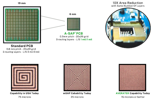
ASC is ready to bring you the future. In this newsletter we are proud to present our new Ultra HDI technology which allows us to produce PCBs with parameters never seen before in our industry. Imagine lines down to 1 mil with a line aspect ratio of 1:1 at production volumes.
These technologies will no longer be what you might fondly call “science projects” in a prototyping phase but rather part of our daily portfolio of offerings.

If your product needs are:
  • Interposer or package substrates
  • Medical devices. Our A-SAP™ licensed process produces biocompatible copper and nickel free circuits
  • Semiconductor test equipment
  • Any other products requiring the densest circuitry and BGAs available today

Call us and we'll talk to you about your special project.

In the meantime, read on to find out more about this cutting-edge technology below.

As always, we thank you for your business.

Sincerely,

Anaya Vardya
President and CEO
American Standard Circuits
Upcoming Webinars
Talking DFM - Design Software

This webinar is a live Q&A between a PCB Designer & ASC. The discussion will be from a PCB Designer & Fabricator perspective and how to best optimize for the lowest cost for performance.
March 8, 2023 11AM Central Time
(US and Canada)
Advanced Flex / Rigid-Flex Circuits: A Focus On Electricals

Flex and rigid flex are a significantly growing portion of the global PCB market. This webinar presented by Geoffrey Leeds of Insulectro will be a continuation from our last month's discussion on the material science of flex & Rigid-Flex. We will cover the physics! Specifically, the electricals. Signal integrity and flex: dielectrics, cross-hatch ground planes, bonded multilayer cables or loose leaf How do these factors affect your designs? How should you make a decision? Join this webinar to understand more of the fundamentals and bend the rules of PCB design to make Flex-PCB's perform.

March 15, 2023 11AM Central Time

What Are The Benefits Of A-SAP™ Technology? 

American Standard Circuits has partnered with Averatek on their A-SAPTM technology (Averatek-Semi Additive Process). This additive process (as opposed to the current subtractive process) allows PCB manufacturing with line width and space down to 15 microns (0.6 mils). Some of the benefits of using A-SAPTM are:
  • Significant size & weight reduction
  • Improved reliability & signal integrity
  • Improved RF performance
  • Reduced costs
  • Biocompatibility
Printed Circuit Manufacturing costs are reduced by reducing the PCB footprint size, number of layers and number of lamination cycles. The key chemical component of the process is LMITM (Liquid Metal Ink), which produces a thin, uniform, and dense electroless deposition. Features of LMITM deposit include:
  • Ultra thin: a few nanometers thick
  • Ultra dense: fully-packed atomic film
  • Conforms to any 3D surface at a nanometer scale
  • Non-Aqueous: enables low-cost manufacturing
  • Works for many different pure metals and alloys of those metals: copper, gold, silver, palladium, platinum, etc.


ASC Experts - Interview on the A-SAP™ Process
Steve Williams sits down with John Johnson to discuss the licensed A-SAP™process that ASC uses to manufacture 25 micron ultra high density interconnects.
Our Free E-Books:
17,000 Downloads and Counting!
Flex and Rigid-Flex Fundamentals

Fundamentals of RF/Microwave PCBs

PCB Fundamentals

Thermal Management: A Fabricators Perspective                 
Our Experts are one reason why American Standard Circuits is North America's leading independent PCB fabricator. Our entire experienced and professional staff is ready and able to make your next PCB project easy!