|
Keith Mitchell,
IT Systems/Web Administrator
Sept. 2 (26 Years)
|
|
October 20-25, 2019
Columbus, OH
Website
22nd International Conference on Secondary Ion Mass Spectrometry (SIMS-22)
October 20-25, 2019
Kyoto, Japan
AVS National Short Course Program
October 21-24, 2019
Columbus, OH
Notice of 28th Plenary Meeting of ISO/TC 201 and meetings of its subcommittees (Tsukuba Meeting): Surface Chemical Analysis
October 31-November 2, 2019
Tsukuba, Japan
International Symposium on Clusters and Nanomaterials
November 3-7, 2019
Richmond, VA
TACT 2019 International Thin Films Conference (TACT2019)
November 17-20, 2019
Taipei, Taiwan
Workshop on Innovative Nanoscale Devices & Systems (WINDS)
December 1, 2019
Kohala Coast (Big Island), HI
2019 MRS Fall Meeting & Exhibit
December 1-6, 2019
Boston, Massachusetts
The 3rd International Symposium of the Vacuum Society of the Philippines
January 8-10, 2020
Cebu, Philippines
47th International Conference on the Physics and Chemistry of Semiconductor Interfaces (PCSI-47)
January 19-23, 2020
B
oulder, Colorado
Website
Area Selective Deposition Workshop
April 2-3, 2020
Stanford, California
International Conference On Metallurgical Coatings & Thin Films (
ICMCTF'20)
April 26-May 1, 2020
San Diego, California
Website
20th International Conference on Atomic Layer Deposition (ALD 2020)
June 28-July 1, 2020
Ghent, Belgium
Website
Atomic Layer Etching Workshop (ALE 2020)
June 28-July 1, 2020
Ghent, Belgium
Website
AVS 67
October 25-30, 2020
Denver, Colorado
Website
Pacific Rim Symposium on Surfaces, Coatings, & Interfaces (PacSurf 2020)
December 6-10, 2020
Waikoloa, Hawaii
Website
|
|
Columbus, Ohio (
In conjunction with the AVS 66th International Symposium & Exhibition)
Sunday, January 26, 2020
Cary, North Carolina
Sunday, April 26, 2020
San Diego, California (In conjunction with the International Conference on Metallurgical Coatings and Thin Films)
Monday, July 27, 2020
N
ew York, New York (In conjunction with a visit to AVS HQ)
Sunday, October 25, 2020
Denver, Colorado
(In conjunction with the AVS 67th International Symposium & Exhibition)
|
|
Massachusetts Institute of Technology (MIT)
Ecole de technologie superieure
"We phone screened 30-40 candidates and face-to-face interviewed - 15 from resum
es received via the AVS job posti
ngs online.
We hired 3 of those. I also attended the AVS
conference in Nashville to recruit at the job fair and hired one engineer from that trip."
-
James Paris, Hitachi High Technologies America
"The AVS Career Center was very helpful when I needed to quickly get qualified experienced candidate resumes for a recent opening. Our position was filled by an applicant who saw our posting on the AVS Job Openings web page." -Larry Gilbert, Vacuum Solutions Group
|
|
|
ABBESS Instruments
American Institute of Physics
ANCORP
Anderson Dahlen - Applied Vacuum Technology
Busch Vacuum Pumps and Systems
Challentech International Corp.
COSMOTEC, Inc.
Denton Vacuum, LLC
Duniway Stockroom Corp.
Ebara Technologies, Inc.
Edwards Vacuum, Inc.
EP Laboratories, Inc.
Gamma Vacuum
Helium Leak Testing, Inc.
Hiden Analytical, Inc.
HIS Vacuum Solutions
ION-TOF USA Inc.
Kurt J. Lesker Company
Luxel Corporation
Mack Vacuum
Technologies
, Inc.
MDC Vacuum Products, LLC
MKS Instruments, Inc.
Nordiko Technical Services Limited
Optiforms, Inc.
Pfeiffer Vacuum Technology
Physical Electronics
Plasmaterials
Plasma
-Therm
Precision Plus Vacuum Parts
Process Materials, Inc.
Provac Sales, Inc.
Quantum Innovations, Inc.
R.D. Mathis Company
RBD Instruments, Inc.
Reynard Corporation
RF VII, Inc.
SPECS Surface Nano Analysis GmbH
SPI Supplies
Staib Instruments, Inc.
Sumitomo (SHI) Cyrogenics of
America
, Inc.
Super Conductor Materials, Inc.
SynSysCo
Thermo Fisher Scientific
For more information on the benefits of becoming a Corporate Member, please contact Angela Klink, 212-248-0200, ext. 221 or visit www.avs.org.
|
|
|
|
|
|
|
Reminder to View your AVS Membership Information
|
 MyAVS allows you to edit your contact information, update your Society demographics (including Chapter and Division information), verify if you are a current AVS member, check when your membership is about to expire, as well as access all your Society benefits. Simply Login to MyAVS with your e-mail address and a password that you have set up. To review your contact and demographic information, on the left hand navigation menu under MyAVS Account, select Edit My Info, then click on Edit/View Information
. MyAVS allows you to edit your contact information, update your Society demographics (including Chapter and Division information), verify if you are a current AVS member, check when your membership is about to expire, as well as access all your Society benefits. Simply Login to MyAVS with your e-mail address and a password that you have set up. To review your contact and demographic information, on the left hand navigation menu under MyAVS Account, select Edit My Info, then click on Edit/View Information
.
|
|
Give the Gift of AVS Membership to a Student
|
Looking for the perfect gift for your student? Consider an act of mentorship by gifting your student an AVS 2019 Membership. For $40 you'll be giving your student great AVS Benefits.
AVS Membership will build your student's network with their peers as well as professionals in the field. Your gift includes key resources that can quickly help them transition into the professional world. Simply tell us the name of the student and complete our quick and easy
GIFT FORM
to give the gift of professional networking.
|
|
AVS 66 SYMPOSIUM HIGHLIGHTS
|
|
Symmetries in Physical Systems Help Optimize Quantum Computing
|
Presentation: "Mapping Quantum Systems to Quantum Computers using Symmetry,"
Daniel Gunlycke, S. Fischer, C.S. Hellberg, S. Policastro, S. Tafur, U.S. Naval Research Laboratory
Monday, October 21, 8:40 a.m.
Reducing unintentional entanglement effects using the symmetries in a system will improve accuracy in quantum computing.
Quantum entanglement has important applications in quantum information science and quantum computing, but unintentional quantum entanglement can lead to a variety of undesirable consequences.
At the AVS 66th International Symposium and Exhibition, Daniel Gunlycke, a theoretical physicist at the U.S. Naval Research Laboratory, will present a study on using symmetry to reduce the effects of random quantum entanglement in quantum computing applications.
While deliberate, quantum entanglement can make algorithms more powerful and efficient, uncon
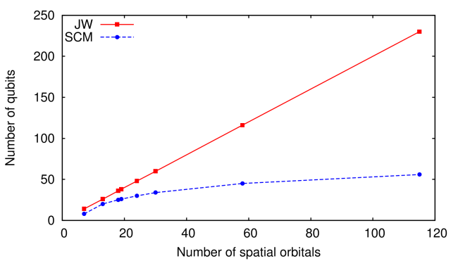 trolled entanglement adds unnecessary additional complexity to quantum computing, making algorithms suboptimal and more prone to error. By reducing the frequency of accidental entanglements, quantum computing can be improved.
Currently, more computational space is allotted to quantum computing jobs than necessary, according to the researchers. A major drawback is the potential for entangled noise to couple states into unassigned space, leading to glitches in the computations.
"This would not be an issue if the calculations were perfect," Gunlycke said. "However, because our existing noisy intermediate-state quantum computers introduce unintended entanglement into our calculations, there is a finite probability that a physical state is mapped to an unintended part of the computational space, resulting in computational errors."
To address this, Gunlycke and his collaborators have developed a new method that reduces the computational space required, decreasing the possibility of errors caused by accidental entanglement.
The more symmetry a system has, the fewer quantum states it requires, and the smaller its allotted computational space can be. Gunlycke's method taps into the symmetry of a physical system to map the system's states into computational space, thereby assigning an appropriate amount of space to each computation.
"Our target-customized mappings require a lot more classical pre- and post-processing," Gunlycke said. "That, however, is a small price to pay for the improved effectiveness of our quantum computations."
|
Improving Optical Characteristics of Thin Glass
|
Presentation:"Characterization of Glass and Durable Optical Surfaces and Their Modes of Failure"
Albert Fahey, D. Baker and T. Dimond, Corning Inc.
Thursday, October 24, 2:20 p.m.
Modern advances in glass manufacturing have led to improvements in how we interact with personal electronic devices.
In recent years, glass has become an important part of our day-to-day lives, acting as the boundary between humans and how we interact with information and communication.
At the AVS 66
th International Symposium and Exhibition in Columbus, Ohio, Albert Fahey, an associate scientist at Corning Incorporated, will give a talk on the methods used to study the chemical and mechanical properties of glass and other optical surfaces.
Modern technologies' reliance on advances in glass have led to new requirements placed on the development of the material. For example, for applications in information displays, there is a need for surfaces that are bright and show high definition but are simultaneously durable.
"This is a modern approach to doing something that's thousands of years old," said Fahey. "It's made of dirt, but it's elevated to a high-tech material."
Because the bulk material that allows devices to have properties like high-definition displays is below the glass surface, part of the challenge in manufacturing the glass lies in making it both thinner - which has also led to improved touchscreen sensitivity - and stronger.
"It has to be workable and free of defects," Fahey said. "We have to make these things last and survive regular consumer abuse."
The near-surface region of the glass also plays a key role in how we interact with it. Scratch resistance, reflectivity, cleanability and appearance are all characteristics of the glass that depend on its structure at its surface.
"A lot of chemistry is involved in the top 50-100 nanometers," said Fahey. "This is where surface and microanalysis come in. Chemical variations play an important role."
Fahey and his team are also trying to bring awareness to the effects of anti-reflectivity on energy efficiency. Anti-reflective coatings allow consumers to view devices from a wide range of angles with relatively low reflection.
"If there's less of a reflection, the screen doesn't have to be quite as bright," he said. "This can help extend battery life."
In his talk, Fahey will discuss how scientists are working to better understand these optical surfaces and their limits, and what new things are being done to improve user friendliness.
|
Studying Ice to Understand Astrophysical Bodies
|
Presentation: "Molecular Processes on Icy Surfaces in the Interstellar Medium and the Outer Solar System"
Edith Fayolle, R. Hodyss, P. Johnson, Jet Propulsion Laboratory, California Institute of Technology; K. Oberg, Harvard University; J-H. Fillion, M. Bertin, Sorbonne Université
Friday, October 25, 10:00 a.m.
Simulating the formation and evolution of ice in astrophysical systems will help scientists understand stellar and planetary composition.
Ice has been observed in a variety of different types of astrophysical environments, from the moon's polar craters to the interstellar medium and the ice crusts of planets on the outer end of our solar system. Understanding the formation and evolution of this ice can provide information about the physical conditions encountered in space and the chemical similarities and differences between planetary and stellar systems.
At the AVS 66th International Symposium and Exhibition in Columbus, Ohio, Edith Fayolle, an astrochemist at NASA's Jet Propulsion Laboratory, will talk about how scientists are trying to understand ice formation, sublimation and composition on astrophysical bodies.
"It informs us about the conditions pertaining to star-forming environments, and it helps us understand whether the chemical complexity observed in our solar system is unique or not," said Fayolle.
To fill this gap in knowledge, Fayolle and her colleagues reproduce astrophysical conditions to grow ice in a lab and study some of its fundamental parameters. By using vacuum and cryogenic techniques along with energy sources, they simulate the conditions encountered during stellar and planetary formation and study the ice composition and evolution of these systems.
It is not possible to reproduce every aspect of a space system in a lab, and Fayolle noted these experiments come with several shortcomings. While the researchers are able to create space temperature conditions in the lab, they cannot achieve the low pressures found in star forming regions. Additionally, time presents a problem.
"Processes usually take 100,000 of years in space," Fayolle said. "The time scales are very different." In the lab, an experiment can only run for a couple of hours.
In her talk, Fayolle will discuss these challenges and present examples of astrochemical experiments relating to icy space environments. Results from these experiments will provide scientists with parameters to use as inputs in modeling various types of astrochemical bodies, which can help explain some surprising recent astrophysical observations.
|
Growth of Pulsed Laser Deposited Few-layer WS2 Films
|
Urmilaben P. Rathod, Bimin Cai, Chukwudi Iheomamere, Gilbert Nyandoto, Andrey A. Voevodin, and
Nigel D. Shepherd
Journal of Vacuum Science and Technolog
y A,
Vol.
37, 051505
(2019)
X-ray photoelectron, Raman, and diffraction studies of few-layered pulsed laser deposited WS
2 films were performed as a function of laser fluence and frequency to understand the impact on structure and properties. Supersaturation of the growth surface created by high fluence was conducive to nucleation and growth, but the obtained films were sulfur deficient. Sulfur desorption at high fluence is due to large kinetic energy transfer and energetic peening of the growing film from the impinging flux. Loss of sulfur was also observed at low frequency where the off period of the supply flux was relatively large. With improvement of the S/W ratio from 1.1 to 1.8, the mobility increased from 0.1 to 6.5 cm
2
V−1
s−1
, while the associated change in the electron sheet concentration followed the opposite trend. Annealing at high temperature under conditions that conserved stoichiometry dramatically improved the crystallinity and further improved the mobility from 6.5 to 19.5 cm2
V−1
s−1
. The correlations between structure, Hall mobility, and Fermi level positions indicate that reducing chalcogen vacancies is critical for optimal mobility in all pulsed laser deposited transition metal dichalcogenide films.
 Read More
|
|
Oxygen Reduction Reaction Mechanism of N-doped Graphene Nanoribbons
|
Haruyuki Matsuyama, Shun-ichi Gomi, and Jun Nakamura
Journal of Vacuum Science and Technology B,
Vol
.
37
, 041803 (2019)
The oxygen reduction reaction (ORR) activity for the N-doped graphene nanoribbons with armchair (N-ACGNRs) and zigzag (N-ZZGNRs) edges has been investigated using first-principles calculations within the density functional theory. The values of the maximum electrode potential (U
Max
) for each doping site and reaction site of N-ACGNRs and N-ZZGNRs have been calculated. The selectivity for ORR with respect to two pathways, the direct four-electron (4e
−
) and the two-electron (2e
−
) pathways, has also been examined. The U
Max
for N-ZZGNR has a parity dependence with regard to the nitrogen doping site in the vicinity of the zigzag edge: For the even-numbered doping sites from the edge, the values of U
Max
are larger than 0 V, while for the odd-numbered ones, those become negative. On the other hand, the U
Max
for N-ACGNR becomes positive for each doping and reaction site. The reaction selectivity for the 4e
−
pathway appears only in the vicinity of the edges for N-ACGNRs and N-ZZGNRs, because the reaction intermediates adsorb stably on the edge C or π
*
-localized C atom adjacent to the doped N atom.
Read More
|
|
Layer-by-layer Constructed Hyaluronic Acid/Chitosan Multilayers as Antifouling and Fouling-release Coatings
|
Wenfa Yu, Julian Koc, John A. Finlay, Jessica L. Clarke, Anthony S. Clare, and Axel Rosenhahn
Biointerphases 14, 051002 (2019)
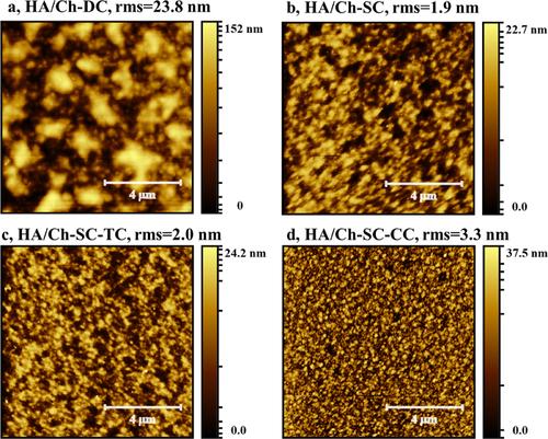 Polyelectrolyte multilayers (PEMs) consisting of hyaluronic acid (HA) and chitosan (Ch) are extensively studied for biomedical applications and suppress bacterial and protein attachment. Here, we prepared and tested HA/Ch PEMs as marine fouling-release coatings. PEMs were constructed by layer-by-layer a
ssembly using spin coating. The multilayers were crosslinked for enhanced
stability in the sea water environment by chemical and thermal treatment. Protein-repelling properties of the crosslinked multilayers were investigated by surface plasmon resonance spectroscopy. The marine antifouling and fouling-release properties were tested against the settlement of zoospores of the green alga Ulva linza and the subsequent development and removal of sporelings. With spin coating and thermal crosslinking, a thick yet homogeneous coating was obtained with antifouling properties against marine algal zoospores indicating the potential of these compounds for application in protective coatings.
Polyelectrolyte multilayers (PEMs) consisting of hyaluronic acid (HA) and chitosan (Ch) are extensively studied for biomedical applications and suppress bacterial and protein attachment. Here, we prepared and tested HA/Ch PEMs as marine fouling-release coatings. PEMs were constructed by layer-by-layer a
ssembly using spin coating. The multilayers were crosslinked for enhanced
stability in the sea water environment by chemical and thermal treatment. Protein-repelling properties of the crosslinked multilayers were investigated by surface plasmon resonance spectroscopy. The marine antifouling and fouling-release properties were tested against the settlement of zoospores of the green alga Ulva linza and the subsequent development and removal of sporelings. With spin coating and thermal crosslinking, a thick yet homogeneous coating was obtained with antifouling properties against marine algal zoospores indicating the potential of these compounds for application in protective coatings.
Read More
|
|
Improved Ion Imaging of Slowly Dried Neurons and Skin Cells by Graphene Cover in Time-of-flight Secondary Ion Mass Spectrometry
|
Sun Young Lee, Heejin Lim, Dae Won Moon, and Jae Young Kim
Biointerphases 14, 051001 (2019)
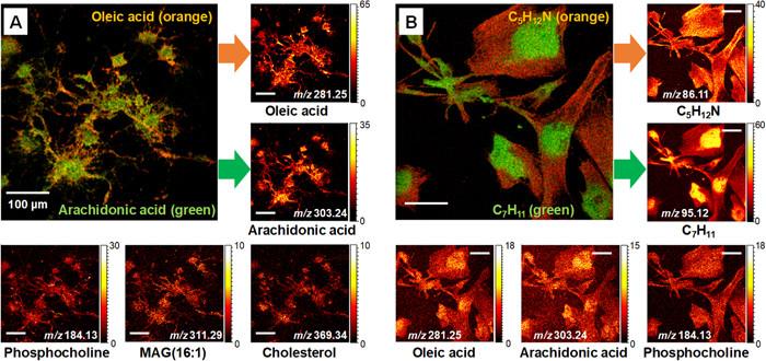 Time-of-flight secondary ion mass spectrometry (ToF-SIMS) is a powerful tool to obtain both chemical information and spatial distribution of specific molecules of interest on a specimen surface. However, since the focused ion beam requires ultrahigh vacuum conditions for desorption and ionization of analytes, proper specimen preparation, such as drying, freeze-drying, and frozen dehydration, is required for ToF-SIMS analysis. In particular, biological specimens with high moisture content generally have a problem of specimen deformation during the normal drying process for a vacuum environment. In this study, the authors propose a cellular specimen preparation method to improve the ion imaging of cells by reducing the deformation of specimens in ToF-SIMS analysis. When the cells on the slide substrate are completely covered with single-layer graphene, the ToF-SIMS imaging is improved by reduced cell deformation due to slow drying. In addition, the graphene encapsulation also induces a reduction in the yield of secondary ions, thereby suppressing the background ion spectra generated by the unwanted organic residues on the substrate, resulting in the improvement of ToF-SIMS imaging. The authors also found that adding plasma treatment to this sample preparation can further improve ion imaging of cells. After cell dehydration is completed, the covered graphene layer can be peeled off by air-plasma treatment and the unwanted organic residues on the substrate can be removed due to plasma cleaning, thereby much improving ion imaging of cells.
Read More
Time-of-flight secondary ion mass spectrometry (ToF-SIMS) is a powerful tool to obtain both chemical information and spatial distribution of specific molecules of interest on a specimen surface. However, since the focused ion beam requires ultrahigh vacuum conditions for desorption and ionization of analytes, proper specimen preparation, such as drying, freeze-drying, and frozen dehydration, is required for ToF-SIMS analysis. In particular, biological specimens with high moisture content generally have a problem of specimen deformation during the normal drying process for a vacuum environment. In this study, the authors propose a cellular specimen preparation method to improve the ion imaging of cells by reducing the deformation of specimens in ToF-SIMS analysis. When the cells on the slide substrate are completely covered with single-layer graphene, the ToF-SIMS imaging is improved by reduced cell deformation due to slow drying. In addition, the graphene encapsulation also induces a reduction in the yield of secondary ions, thereby suppressing the background ion spectra generated by the unwanted organic residues on the substrate, resulting in the improvement of ToF-SIMS imaging. The authors also found that adding plasma treatment to this sample preparation can further improve ion imaging of cells. After cell dehydration is completed, the covered graphene layer can be peeled off by air-plasma treatment and the unwanted organic residues on the substrate can be removed due to plasma cleaning, thereby much improving ion imaging of cells.
Read More
|
|
AVS Offers Discount on Long-term Care Insurance
|
No longer being able to care for yourself isn't something anyone wants to think about, but many will need some form of long-term care services.
The average out of pocket cost for assisted living is quite high. AVS is
offering a discount for Long-Term Care Resources (LTCR) to bring you
LTCRplus
, a program that provides assistance throughout these key areas of long-term care planning:
- Funding
- Navigation
- Care Audit
- Legal
|
|
AVS 66 Store, Booth #734, Exhibit Hall
|
Official AVS logo items including graphic tees and other merchandise will be available for purchase throughout the week. Stop by and see the new AVS 65 T-shirt contest winning shirt which will be available for purchase.
|
|
AVS 66th International Symposium and Exhibition
|
October 20-25, 2019
Columbus, Ohio
Housing and Registration is Now Open
The AVS 66th International Symposium and Exhibition will be held October 20-25, 2019, at the Greater Columbus Convention Center, in Columbus, Ohio. Highlights include an extensive collection of technical and poster sessions, professional development activities, and a free to attend equipment exhibition.
This year's annual meeting theme is "Shaping Our Future: Materials, Technologies, and Processes for Energy Transition." Exciting sessions that will encompass this year's theme are being planned in the following topical areas:

Plenary Lecture "Roles of Surface and Materials Science in the Direct Production of Fuels from Sunlight," Dr. Nathan S. Lewis, George L. Argyros Prof. of Chemistry, California Institute of Technology
We are developing an artificial photosynthetic system that will utilize sunlight and water as the inputs and produce hydrogen and oxygen as the outputs. We are taking a modular, parallel development approach in which three distinct primary components-the photoanode, the photocathode, and the product-separating but ion-conducting membrane-are fabricated and optimized separately before assembly into a complete water-splitting system. The design principles incorporate two separate, photosensitive semiconductor/liquid junctions that will collectively generate the 1.7-1.9 V at open circuit necessary to support both the oxidation of
H
2
O
(or OH-) and the reduction of H+ (or
H
2
O
). The photoanode and photocathode will consist of rod-like semiconductor components, with attached heterogeneous multi-electron transfer catalysts, which are needed to drive the oxidation or reduction reactions at low overpotentials.
The high aspect-ratio semiconductor rod electrode architecture allows for the use of low cost, earth abundant materials without sacrificing energy conversion efficiency due to the orthogonalization of light absorption and charge-carrier collection. Additionally, the high surface-area design of the rod-based semiconductor array electrode inherently lowers the flux of charge carriers over the rod array surface relative to the projected geometric surface of the photoelectrode, thus lowering the photocurrent density at the solid/liquid junction and thereby relaxing the demands on the activity (and cost) of any electrocatalysts. A flexible composite polymer film will allow for electron and ion conduction between the photoanode and photocathode while simultaneously preventing mixing of the gaseous products. Separate polymeric materials will be used to make electrical contact between the anode and cathode, and also to provide structural support. Interspersed patches of an ion conducting polymer will maintain charge balance between the two half-cells.
AVS 66 Yoga Classes
Monday, October 21 and Tuesday,
October 22
6:00 a.m.-7:00 a.m.

AVS 66 is offering attendees the opportunity to register for our Yoga Classes. These classes are great for beginners to advanced yogis! Experience completeness of your practice by integrating breath and movement to create a powerful and stabilizing, yet delicate meditative flow.
The measured pace supports quality of breath, postural alignment, and awareness of the body and mind. Experience deep relaxation at the conclusion of our practice together through Guided Visualization Meditation. You will be instructed to form relaxing mental images while incorporating your senses. The sense of peace and balance that meditation provides benefits your emotional well-being and your overall health.
AVS 66 Art Zone Nature Photo Contest
Tuesday-Thursday | October 22-24, 2019
We know that the AVS scientific community loves to travel the world. Whether it is for work or pleasure, it is likely that you take photos to capture and commemorate your journey. We would like to see your favorite nature photos. This could include anything from scenic landscapes to wildlife.
E-mail your 8 inch x 10 inch photo to Abby Rizzo,
abby@avs.org
by
October 7, 2019
. Be sure the image is print resolution noting that a jpg file is preferred. Also, you must be attending AVS 66 to submit; only one entry per person. Submissions will be limited to 50 total.
Attendee Judging and Prizes
All photos will be displayed at the AVS 6
6 Equipment Exhibition from Tuesday-Thursday (October 22-24, 2019, Greater Columbus Convention Center, Columbus, Ohio). Attendees will
have the opportunity to vote for their favorite submission throughout the week. First prize ($800), second prize ($500), and third prize ($300) winners (based on voting) will be announced at the Exhibit Finale on Thursday in the Exhibit Hall.
You must be present to win and collect your prize. These winning images may be used in future AVS promotional pieces.
Entry Deadline: October 7, 2019
(E-mail
abby@avs.org
)
AVS 66 Member Center

AVS Member Center
will have activities focused on: Networking - Professional Development -Diversity and Inclusion
There will be several new exciting sessions presented by a STEM careers expert, each addressing valuable topics for different stages in your career. Plus, schedule a personalized 15 minute one-on-one session with a careers expert on any career-related subject. In addition will have our returning sessions. Please review the agenda.
|
|
AVS 66 National Short Course Program
|
AVS 66 National Short Course Program
October 21-24, 2019
A complete schedule of AVS Short Courses is set to take place in Columbus, Ohio from October 21-24, 2019 in conjunction with the AVS 66th International Symposium and Exhibition. Early/Advance registration is strongly encouraged!
|
|
47th Conference on the Physics and Chemistry of Surfaces and Interfaces (PCSI-47)
|

January 19-23, 2020
The 47th Conference on the Physics and Chemistry of Surfaces and Interfaces (PCSI-47) will be held at the Millennium Harvest House Hotel, in Boulder, Colorado, USA, from Sunday afternoon, January 19, through Thursday noon, January 23. The annual PCSI conference is devoted to achieving a fundamental understanding of the physical, chemical, biological, structural, optical, magnetic and electrical properties of surfaces and interfaces. These studies include novel growth processes and interfacial phenomena, new characterization tools, transport, and functionality of the structures for future devices. Generous amounts of discussion time will be included in the program in order to emphasize the workshop character and to stimulate the exchange of new ideas.
Topics
The conference will cover a wide range of topics including the following:
- Atomically Precise Deposition and Etching Methods
- Characterization of interfaces, transport, and optical properties: in situ and in operando
- Defects as Devices (e.g. Quantum Emitters)
- Electronically Reconfigurable Metasurfaces
- Epitaxial Growth Mechanisms
- Magnetism and Spin Transport in Reduced Dimensions, Multiferroics
- Materials for Neuromorphic Computing
- Materials for Quantum Technologies
- Nanoscale Contacts on Semiconductors and Oxides
- Novel Couplings Across 2D and Mixed-Dimensional Interfaces
- OD, 1D, and 2D Materials for Electronics and Photonics
- Organic and Hybrid Electronics
- Semiconductor and Dielectric Heterostructures
- Surface and Interfaces in Energy Storage and Generation
- Topological Materials
|
|
Workshop on Innovative Nanoscale Devices and Systems (WINDS 2019)
|
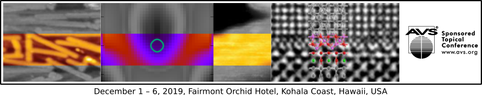
December 1-6, 2019
Fairmont Orchid Hotel
Kohala Coast, Hawaii
The
Workshop on Innovative Nanoscale Devices and Systems (WINDS 2019) covers a spectrum of nanoscale science, emerging materials, and device technologies. The workshop format and setting provide opportunities for significant interactions among participants, including focused individual sessions.
Important Dates:
New Abstract Submission Deadline: October 10, 2019
Special Hotel Rate Deadline: November 1, 2019
Early Registration Deadline: November 18, 2019
The program will consist of invited oral presentations, regular research talks, and a poster session. Participants wishing to give an oral or poster presentation are kindly asked to submit a two-page abstract.
List of confirmed Invited Speakers:
- Chagaan Baatar, Office of Naval Research, USA - Synthetic Electronics
- Kookrin Char, Seoul National University, Republic of Korea - Oxide Electronics
- Claudia Felser, Max Planck Institute, Germany - Materials with High Spin Polarization
- Masataka Higashiwaki, National Institute of Information and Communications Technology, Japan - Gallium Oxide Devices
- Berend Jonker, Naval Research Laboratory, USA - Quantum Calligraphy of Single Photon Emitters and van der Waals / Moire Heterostructures
- Robert Kaplar, Sandia National Labs, USA - Ultra-Widebandgap Materials
- Victor Klimov, Los Alamos National Labs, USA - Colloidal-Quantum-Dot Lasing
- Paolo Lugli, University of Bolzano, Italy - Bioelectronics/Sensors
- Stuart Parkin, Max Planck Institute, Germany - Charge Density Waves
- Eric Pop, Stanford University, USA - 2D Materials for Nanoelectronics
- Joshua Robinson, Pennsylvania State University, USA -- Synthesis and Integration of 2D Materials
- Deepak Singh, University of Missouri, USA - Artificial Honey Comb of Magnetic Spins
- Jairo Sinova, Mainz University, Germany - Spin Hall Effect
- Alex Smolyanitsky, National Institute of Standards and Technology, USA - Ion Channels in 2D Materials
- Tom Soh, Stanford University, USA - Biosensor Technologies
- Masateru Taniguchi, Osaka University, Japan - Quantitative Analysis of DNA with Single-Molecule Sequencing
- Bart van Wees, University of Groningen, Netherlands - Giant Spin Relaxation Anisotropy
- Maia Vergniory, Donostia Int'l. Physics Center, Spain - Topological Quantum Chemistry
- Robert Wallace, University of Texas Dallas, USA - 2D Materials for Nanoelectronics
|
|
International Conference On Metallurgical Coatings & Thin Films (ICMCTF 2020)
|
April 26-May 1, 2020
The ICMCTF is internationally recognized as a vibrant technical conference that integrates fundamental and applied research focused on thin film deposition, characterization, and advanced surface modification techniques. ICMCTF is the premier international meeting in the field promoting global exchange of information among scientists,
technologists, and manufacturers. The conference draws more than 800 attendees each year with multiple oral technical sessions and a well- attended poster session which is a major component of the technical program.
Topics
The conference will cover a wide range of topics including the following:
- Coatings for Use at High Temperatures
- Hard Coatings and Vapor Deposition Technologies
- Fundamentals and Technology of Multifunctional Materials and Devices
- Coatings for Biomedical and Healthcare Applications
- Tribology and Mechanical Behavior of Coatings and Engineered Surfaces
- New Horizons in Coatings and Thin Films
- Surface Engineering - Applied Research and Industrial Applications
- Advanced Characterization Techniques for Coatings, Thin Films, and Small Volumes
- Anti- and De-icing Surface Engineering
- New Horizons in Boron-Containing Coatings: Modeling, Synthesis and Applications
- In-Silico Design of Novel Materials by Quantum Mechanics and Classical Methods
- Photocatalytic and Superhydrophilic Surfaces
- Thin Films on Polymer Substrates: Flexible Electronics and Beyond
|
|
|