Polishing --- Surface Treatment Techniques for Ceramic Substrates Before Printing

As the integrated circuit and semiconductor industries continue to grow rapidly, ceramic substrates with high surface precision and low roughness have become the preferred choice for packaging substrates. Among the production steps, the polishing process is critical to ensuring the overall quality of ceramic substrates.

Polishing Techniques Overview


To enhance flatness and achieve high surface precision and low roughness, ceramic substrates undergo grinding to remove surface defects and scratches. Polishing is then used to eliminate subsurface damage caused by grinding, creating a smooth, low-roughness surface. Common polishing techniques include:

2272-202403011513338333 image

https://www.researchgate.net/

1. Chemical Mechanical Polishing (CMP)

CMP combines chemical corrosion with mechanical removal, achieving nanometer-level precision and sub-nanometer roughness. It uses a synergistic process involving polishing slurry and pads to remove material efficiently while minimizing subsurface damage. CMP is a mainstream method for achieving global planarization on ceramic substrates.

Figure_203-Semiconductor_Handbook_800w image

https://www.mks.com/mam/celum/celum_assets/Figure_203-Semiconductor_Handbook_800w.jpg

2. Magnetorheological Polishing (MRF)

MRF utilizes a magnetic field to control abrasive particles suspended in a fluid. It delivers high precision and low surface roughness, making it ideal for precision optics and small-diameter components.

https://www.researchgate.net/figure/Schematic-of-magnetorheological-finishing-of-ZrO2-ceramics-reused-with-permission-from_fig1_358437996

3. Ultrasonic Vibration-Assisted Abrasive Flow Polishing (UVAFP)

By combining ultrasonic vibrations with abrasive flow, this method enhances surface polishing. The ultrasonic system generates micro-bubbles that collapse and aid material removal, making UVAFP particularly suited for high-precision optical components.

https://link.springer.com/article/10.1007/s00170-021-06666-7

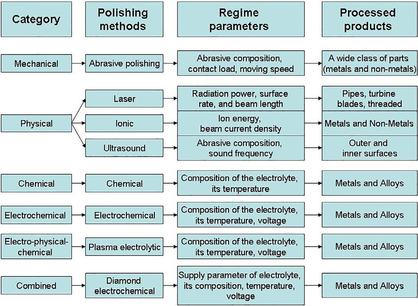
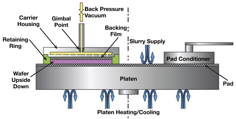
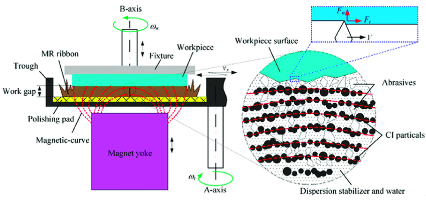
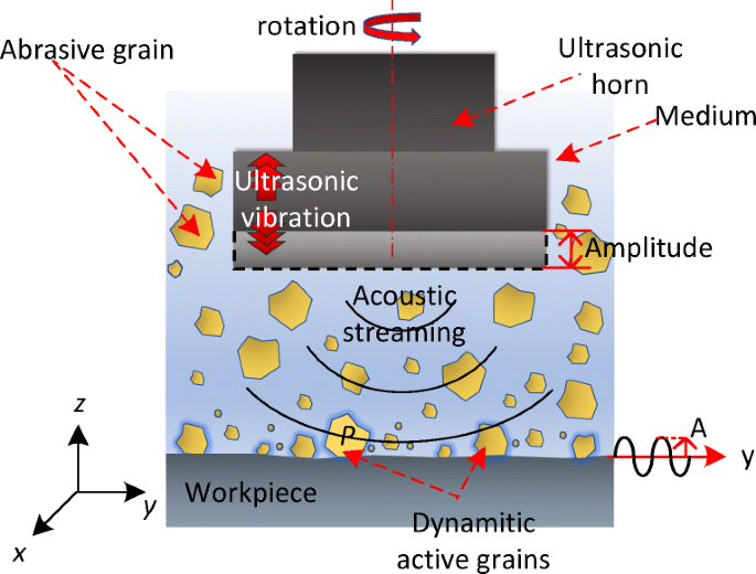
4. Electrophoretic Polishing

Electrophoretic polishing employs charged particles in an electric field to create a flexible abrasive layer. The technique is highly effective for ultra-precision machining of functional ceramics without introducing mechanical damage.


5. Electrolytic Polishing

Electrolytic polishing smooths surfaces by dissolving material through selective anodic reactions. It reduces surface roughness efficiently and enhances corrosion resistance, especially for areas inaccessible by mechanical polishing.


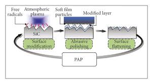
6. Plasma-Assisted Polishing (PAP)

PAP integrates chemical modification and mechanical removal, achieving atomic-level flatness with minimal subsurface damage. This technique excels in processing hard-to-machine ceramics like SiC and AlN.

https://www.researchgate.net/figure/Plasma-assisted-polishing-principle-89_fig27_360562564

Ceramic substrates are foundational materials in integrated circuits and copper-clad boards. Their surface quality directly impacts the performance and reliability of downstream devices. As miniaturization and integration demands grow, stricter requirements for surface treatment will emerge, driving advancements in polishing techniques. Selecting the appropriate polishing method—or a combination thereof—based on the substrate’s material and requirements will remain crucial.

aurel-c920 image

Screen Printer/ Screen Printing line


  • Up to 20 μm with 100 μm standard
  • 400*400 available
  • Manual, auto, semi-auto available
For more information about our belt furnace offerings, please see us at https://www.beltfurnaces.com/furnaces.html

If you want to learn more about our belt furnace, thick film product line, GTMS, LTCC and more,

please leave a message and click here.

Please forward this email to your friends or anyone who you think they might need or like it.


Was this email forwarded to youSign up for our newsletter at our main page!


Looking for HeatsinksClick here - Standard Sizes and more

Looking for MaterialsClick Here - Tungsten, Moly & CuW


Facebook  Twitter  Linkedin  Youtube