Read Recent

Collection on CHIPS:

Future of Semiconductor Processing and Devices

Read the Collection for FREE for a Limited Time!

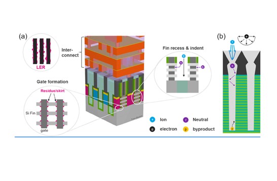
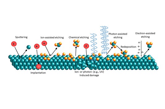
Future of plasma etching for microelectronics: Challenges and opportunities

Gottlieb S. Oehrlein et al.

JVST B 42, 041501 (2024)

READ PAPER

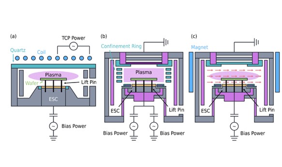
Science challenges and research opportunities for plasma applications in microelectronics

David B. Graves, Catherine B. Labelle, Mark J. Kushner, Eray S. Aydil, Vincent M. Donnelly, Jane P. Chang, Peter Mayer, Lawrence Overzet, Steven Shannon, Shahid Rauf, and David N. Ruzic

JVST B 42, 042202 (2024)

READ PAPER

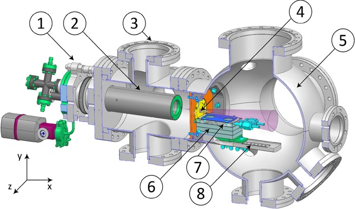
Novel low-temperature and high-flux hydrogen plasma source for extreme-ultraviolet lithography applications

A. S. Stodolna, T. W. Mechielsen, P. van der Walle, C. Meekes, and H. Lensen

JVST B 42, 052601 (2024)

READ PAPER

In situ plasma pin-up clean process for backside bevel polymer removal, defect reduction, and queue time relaxation

Benjamin B. Ye, Ganquan Song, and Jeff J. Ye

JVST B 42, 022202 (2024)

READ PAPER

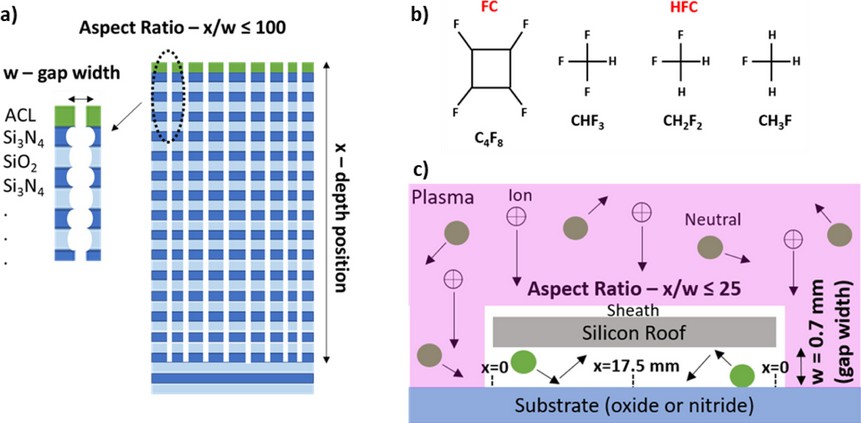
Exploring oxide-nitride-oxide scalloping behavior with small gap structure and chemical analysis after fluorocarbon or hydrofluorocarbon plasma processing

Sang-Jin Chung, Pingshan Luan, Minjoon Park, Andrew Metz, Gottlieb S. Oehrlein

JVST B 41, 062201 (2023)

READ PAPER

- PUBLISHED BY -

 
X  Facebook  Linkedin  Instagram  Youtube