|
‘SUSTAIN AND SECURE’: As USACA grows, we are re-dedicating our efforts to influence federal science and technology funding and industrial base investments and shape national priorities to close gaps America’s global competitiveness in ceramics technologies.
USACA Technical Director Dr. Haynes, fresh off an illustrious Pentagon career transitioning emerging technologies to the field, offered attendees in Colorado a bird’s eye view of her plans to “sustain and secure USACA’s role as leader in advancing ceramics industrialization.”
She will be convening dedicated meetings with member companies and universities, conducting new surveys on member needs and objectives, developing the technical agenda for the 2026 Composites, Materials, and Structures (CMS) conference, increasing USACA’s government visibility, and crafting our longer-term roadmap, including a U.S. Advanced Ceramics Strategy with vision for the next 20 years.
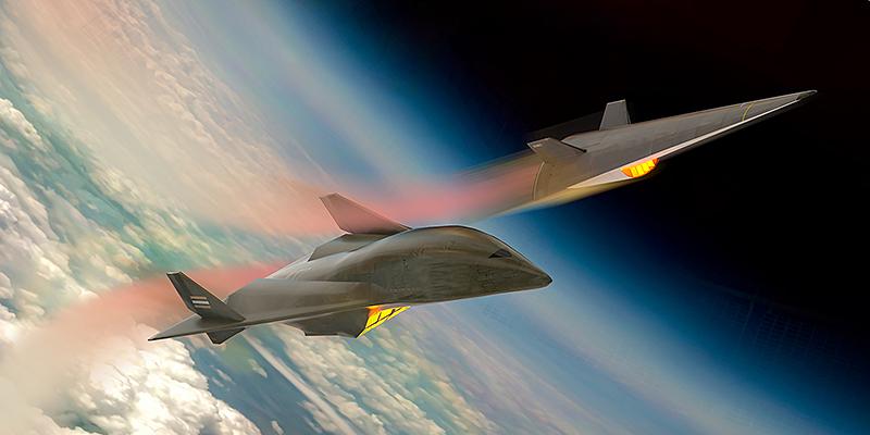
Priority areas: Dr. Haynes outlined a series of more robust focus areas at the Department of War and other federal agencies that are relevant to USACA, including accelerating materials through AI and autonomous experimentation, advanced manufacturing, microelectronics, communications, and quantum computing.
The need for speed: Paramount will be the government’s new intent to be “aggressive in execution and accelerating timelines,” she said, including turning to multiple suppliers with domestic production capacity.
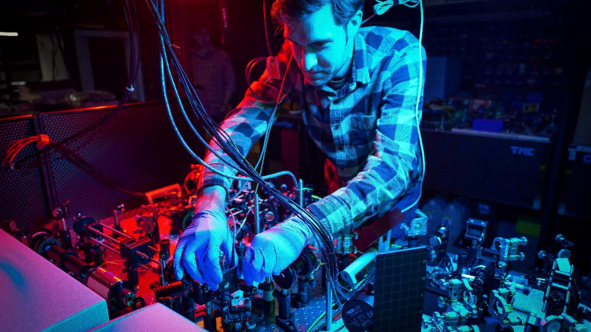
QUANTUM LEAP: Speaking of quantum computing, special thanks to Corban Tillemann-Dick, founder and CEO of Maybell Quantum Industries, who delivered a timely and illuminating presentation at the fall meeting on how “quantum technologies will be as important to the next century as the integrated circuit was to the last century.”
He explained how quantum computing will transform a host of industries and technical disciplines, including engineering, aerospace, materials, transportation, climate, energy, biotechnology, and national security.
Warning shot: But he also stressed that the United States is behind the curve in embracing the possibilities and making both the public and private investment necessary to lead. This is another area where we are trailing China, which is well on its way to “complete supply chain development.”
That is translating into large projects that require “building entire domestic ecosystems of specialized suppliers, creating dependencies that are nearly impossible for competitors to replicate quickly.” Beijing is also training technicians, engineers, and project managers to create “a knowledge base that becomes a national strategic asset.”
FINGER ON THE PULSE: USACA prides itself on being a forum for industry and academic practitioners to interact directly with current and former government scientists and other technologists who are steering what’s next for federal labs and other government institutions at the forefront of evaluating and validating new materials and manufacturing processes.
Special thanks to Dr. Katie Harrison, a researcher at National Renewable Energy Laboratory, who briefed attendees in Colorado on “Enhanced Validation of Advanced Battery Supply Chain.”
Likewise for Dr. Randy Hay, Principal Materials Research Engineer at the Air Force Research Laboratory, who delivered a presentation on Ceramic Research Opportunities.
‘UNDERLYING MATERIALS.’ The White House Office of Management and Budget recently released the Trump administration’s R&D budget priorities for Fiscal Year 2027.
“Federal investments in semiconductor and microelectronics R&D are critical to enabling the development and deployment of AI and quantum applications and strengthening supply chain resilience,” the memo from OMB Director Russell Vought says. “Agencies, working together and in collaboration with industry and academic partners where appropriate, should prioritize investments to ensure government access to trusted and assured microelectronics and continued American leadership in semiconductor technologies."
It adds: “Efforts should include underlying materials, devices, designs, and software, with particular focus on and coordination of the fabrication and characterization tools and facilities required for next-generation semiconductor technologies.”
Read the full guidance.
|